
Hi!
maria = girl? If, yes you are pretty unique. It's less than five active women here, like 2-3 or so.
Feel welcome and I'll hope the "grabbigheten"(*) will be turned down a bit.
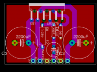
The layout looks good but three things:
1 Add 100 nF/63 V polyester at each power pin, make it as close as possible. You could even "snuibberize" it a la carlsofm. 0.5-1 ohms 0.6 W metal film will do. You could even use SMD 1206 or 0805.
2 Draw the ground trace on the "blue" side and connected it as you have done now.
3 You have to add a zobel network at the output. 2-3 ohms + 100 nF for stability reasons. I recommend that you take a close look at the datasheet and the applcation note AN-1192 from National. You could also take a look at the excellent pcb from Pater Daniel /Brian bell. www.chipamp.com and you may also check my Gainclone and while you're at it, check the Gainclone webring, see below.
*) Någon har ett bra ord för grabbighet? English word for grabbighet?
maria = girl? If, yes you are pretty unique. It's less than five active women here, like 2-3 or so.
Feel welcome and I'll hope the "grabbigheten"(*) will be turned down a bit.
The layout looks good but three things:
1 Add 100 nF/63 V polyester at each power pin, make it as close as possible. You could even "snuibberize" it a la carlsofm. 0.5-1 ohms 0.6 W metal film will do. You could even use SMD 1206 or 0805.
2 Draw the ground trace on the "blue" side and connected it as you have done now.
3 You have to add a zobel network at the output. 2-3 ohms + 100 nF for stability reasons. I recommend that you take a close look at the datasheet and the applcation note AN-1192 from National. You could also take a look at the excellent pcb from Pater Daniel /Brian bell. www.chipamp.com and you may also check my Gainclone and while you're at it, check the Gainclone webring, see below.
*) Någon har ett bra ord för grabbighet? English word for grabbighet?
Thanks for the replys (it means a lot to get qualified help), eitherway I have some questions for you Per Anders and everyone else for that matter.
"Add 100 nF/63 V polyester at each power pin, make it as close as possible", does this mean that I should add a cap from +V to GND as close to the 2200uF cap as possible? The same for -V of course.
"Draw the ground trace on the "blue" side and connected it as you have done now." You mean draw the Signal GND on the blue side and connect it to the gound plane using a via? or draw both Signal GND and Power GND on the blue side, essentially making the PCB singel sided? If the latter applies, is there any reason not to make the PCB double sided (except for cost issues)?
Also I am a bit unsure (I have understood from your previous comments on gainclone PCB contruction at diyaudio.com that you do like this) why you make a small connection between the Signal GND and the Power GND like I have done here. If someone could explain the intended reason. I guess it have something to do with currents in the ground plan.
Zobel network is not understood on my behalf but I reason stability issues are good enough reasons.
I don't know any good translation for "grabbighet" actually, I'll inform you if I find any good word.
Either way, thanks in advance for all help.
"Close as possible" is to the supply pin, the current consumer. You can check my layouts as an example.
Strive to have a whole groundplane (not divided by traces) and strive to keep the signal ground very close to the speaker ground. Bear in mind that you should keep the currents from the smoothing caps away from the signal ground. Strive to have the signal ground as "current free" as possible.
If you check my QRP02 layout you can clearly see how I have isolated the grounds.
Don't forget screwholes in your pcb.
To reduce offset your R2 should be the value as R3 and it's possible that you need to decouple it with 10-100 nF.
Ok, I should try to make reason out of this as soon as I'm home from work. There are still some things I don't understand, but I guess you can confirm my guesses later on via new PCB design. Also, I'll check out you PCBs and see how they apply to mine (I know that your gainclone PCBs use to be quiet loaded with 'features').
I get the idea that you should not devide the ground plane if possible. I suppose you can get currents in the ground plane otherwise. Right/Wrong? I guess the ground plane have sheilding effect on the PCB also.
"Don't forget screwholes in your pcb" I'll mount it using the hole in the IC, like Brian GTs PCBs sort of.
R2 should go from 4.7K to 120K? Right?
As said, I'll re-cad and get back to you guys and we'll see if I have understood what you mean.
Thanks again
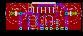
Hello again, (and as always, thanks for all help, it's reall appreciated), here is the new PCB which I have been modifiyng to meet PA ideas/suggestions. I'm quiet aware that I might have missunderstood some parts so please tell me if there are anything that is wrong.
I have some questions though.
I have some questions though.
- What watt rating is sufficient for the Zobel network, is 0.6 watt metal film resistors ok?
- The cap in the Zobel network, would 64 Volts work?
- Does the grounding arrangement look ok? This is really hard to figure out.
- Also, did I understand you correct that the 4.7K resistor should be a 120K resistor instead?
[/list=1]
Ok, I guess I have more questions that I can't come to think of now.
Thanks in advance for all help.
Attachments
Ideally, the inverting input should "see" the same DC resistance as the non-inverting. If so you have eliminated pretty much DC offset.
The gain should be 20-30 if you have normal signals but my recommendation is to start at 20. Don't have more gain than necessary. You will only get more noise.
Rf = 220 K
Rin = 10 k
These are common values but you can choose to have lower.
The only thing I don't like about this configuration is the rather big electrolythic cap at the input. I myself prefer an extremely good buffer AD8620 and a direct connection to the LM3886, see my SMD Gainclone, OK a bit more complicated but why make simple things")
Mr. Maria could you enable your email button so I can get in touch with you?
The gain should be 20-30 if you have normal signals but my recommendation is to start at 20. Don't have more gain than necessary. You will only get more noise.
Rf = 220 K
Rin = 10 k
These are common values but you can choose to have lower.
The only thing I don't like about this configuration is the rather big electrolythic cap at the input. I myself prefer an extremely good buffer AD8620 and a direct connection to the LM3886, see my SMD Gainclone, OK a bit more complicated but why make simple things
Mr. Maria could you enable your email button so I can get in touch with you?
Ok, thanks for the input, I will check out the input buffer.
Per Anders, I don't know how to make the e-mail button appear but you can send a mail to maria.anderssson@gmail.com
Per Anders, I don't know how to make the e-mail button appear but you can send a mail to maria.anderssson@gmail.com
The only thing I don't like about this configuration is the rather big electrolythic cap at the input.
hear, hear.
maria_andersson said:I don't know any good translation for "grabbighet" actually, I'll inform you if I find any good word.
Eager Beaver(s) ?
maria_andersson said:Per Anders, I don't know how to make the e-mail button appear but you can send a mail to maria.anderssson@gmail.com
Button at the top
USER CP -> Edit Option- > Hide Email Address? -> Check NO
Another hot tips is also NOT to write your email in plain text becasue of spam reasons. Better to write name (at) domain dot com, or simply fake it a bit.
Sure, but I still don't like itjacco vermeulen said:hear, hear.
Ok, I found it,
I think Jacco agreed to your idea with the input buffer PA. Does an input buffer like that help to keep the feed from being 'drained' if you use long interconnects? Or is it just a better DC blocker?
P.S. I read your deal on your homepage about the engineering approach to hifi-electronics. I can only agree that less is not always more. I guess people start to rant about this since if less is added then less is too be understood, which I assume is the hard part. D.S.
A living stone, from the Namibia desert and north South Africa.
http://www.mesembs.com/lithops/index.htm
http://www.mesembs.com/lithops/index.htm
- Status
- This old topic is closed. If you want to reopen this topic, contact a moderator using the "Report Post" button.
- Home
- Amplifiers
- Chip Amps
- Feedback on Gainclone PCB layout Wanted