asgorath said:What do you think about using CarlosFM's Snubber 1.1 power supply in place of mauro's power supply? I am sold on the advantages of regulated over unregulated, but not sure if it will change the dynamics.
An externally hosted image should be here but it was not working when we last tested it.
taken from http://www.diyaudio.com/forums/showthread.php?s=&threadid=56106&perpage=10&pagenumber=15
I am listening to the amp with Mauro's revA boards right now. I can tell you honestly it sounds better than any of my "snubberized" GCs. So, I am not sure it really matters. I am quickly running our of board space on my current work, so I really doubt I could get a regulated PS on what I have right now. But that sounds like a great experiment.
Cheers!
Russ
Maybe, I am atthe office right now, but I cobbled enough parts together to make an amp anyhow. ") I just had to scrounge some .3R resistors instead of the .47R. Everything else I had. My rectifer is a little large for the hole spacing, but I made it fit.
I just had to scrounge some .3R resistors instead of the .47R. Everything else I had. My rectifer is a little large for the hole spacing, but I made it fit.
It will be nice to actually build it with parts that fit.
I just had to scrounge some .3R resistors instead of the .47R. Everything else I had. My rectifer is a little large for the hole spacing, but I made it fit. It will be nice to actually build it with parts that fit.
Hi Russ,
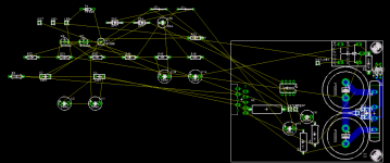
In your circuit it seems me that the track of the contact of the relay (stars GND) is too long and thin, and the bridge is in a "radiant" zone and the run of the +vcc ( radiant even he ) is a little long...
Is not a criticism but a help...
Allow me to listing a brief list of priority that serve you for the construction
of analogical PCB layout. A lot of things for me is obvious because this is a part of my work
professional, but realize me that for a lot of Diy members it my rules are a "abstract" thing.
The specialists of PCB layout is much a few even in "professional" environments ( overall on audio!).
1. The PCB is a " reactive component" that interacts in enormous way with the active electronic circuit.
the principal problems of "trouble" that a layout is able create am:
- Errors of Res serious ( or L serious) in the nodes of the NFB nets.
- EMI emission( toward other sections of the circuit )
- EMI receipt( from other sections of the circuit )
2. To succeed to build a professional layout PCB affair establish un priorities of project.
This priority is a lot of different to second of the type of circuit. in the case of an power amp:
a. Power distribution; To reduce the generation of EMI troubles and increase the efficiency of the
bypass PS (instability reduction) is fundamental have un brief runs and to "root" of the tracks
what am crossed from strong currents. This are: devices power PS, power ground (Hi-caps gnd & spks gnd ),
power devices (to output ) connections. To reduce this crossed it may ( or it is has to) abdicate to the symmetry
of the connectors or of the components. in the case of the GNDs a distribution is had to use to "star", where
the " center star " is " exclusively " the "virtual GND" more strong than the circuit, in our case
it is the GND of the HI-cap (of DC. regulation).
b. PS Bypass; The "overall vision" that is you must be in possession of is that every group of bypass caps integrated on the traces of PS, it is a "node" of short-circuit for the troubles. every section of trace among a node
and the other is a " off- limits "zone , that serve only to transport the energy. Every component activates has to
it is connected to the PS in the point more near possible to the caps "node". A few cm of trace it produces a serious Inductance,
enough to reduce the efficiency of the cap.
c. EMI "isolation" of the circuits " of signal " to low energy ( & input NFB global ). The inputs sections
and of elaboration of the signals have to be positioned in the position more far possible by all the
traces "of power ", in degree to utter troubles for electromagnetic effect. If it is not possible, they are used
of the formed "shield" by tracks or zones of mediate gnd among the two sections. Some components, as the ELS-cap.
of great dimensions are able be of help creditable to the "shielding" effect of their metallic wrap.
d. asymmetrical of the suitable runs and sizing of the traces. I am a lot of diffused the habits to use
ample zones of copper as traces for powers signals or gnd. This technique often is ministerial to increasing it
course of current and the effectiveness of shield, but is possible to create greater "problems". In particular is lost
the follow-up on the runs of the currents, that are clear of " distribute " to second of the internal impedances, and
in some cases produce of the "circulatory" currents that oppose the regular operation. The traces of
power would have to be measured without exaggerate, and with asymmetricals forms that form a "guide" for it currents
. the "shielding" depart (GND) works well only if form of the separated "islands" for Power GND and signal GND.
the points of contact among this islands has to be in an only point, and not crossed by strong currents, otherwise
all the screen becomes a radiant dipole.
The run of the signal has to be brief, but over all doesn't follow parallel lines with "radians" traces ( Power & output tracks).
3. In an power amp the thermic conditionses are important. The positioning of the components has to be account of the
exercise temperatures, leaving space enough to disperse the heat. Besides the actives components ( Power BJTs ) that of
usual am mounted on proper headsink, there are un components as the diodes and the Power res. that often heat. Even the traces
of copper it dissipates the heat ( the really and that of the weld component ). the pads exchange the heat, and have to be measured
in "increased" way.
Besides the active component, that normally cannot work at temperatures superior to 70°C, the components the more sensibles
to the temperatures are the electrolytics caps, that lose rapidly it they characteristic to high temperatures.
Method of project of a power amp PCB layout:
1. Establishing the "thermal" zone ( headsink ) and position the power components.
2. Establishing the run better than the power tracks ( no rings but root ), and of bypass GND. It has to find a jeopardized among
the length of the tracks and the distance of the hi-cap from the headsink. The component the more critical is the diodes bridge and his track.
It has to be much far from the input section, because produces a lot of EMI disturbs. Much put the separate PSU by the amp
for this reason, but the connections wires among the 2 cards create easily of the problems of ground-loop because it is moves
the "virtual gnd". A good method is put the bridge near to the hi-cap. and " hide it " after to their metallic wraps.
3. Positioning the auxiliary components (relay, output choke, etc..) with brief track and far from the circuit of input.
4. positioning the signal circuit ( input & NFB net). It uses short tracks and "recluses" references from the power circuit. The GND signal
has to be an only node or island. Positioning the inputs caps, filters, etc. far from the power circuits because this
nets are un "microphones".
5. positioning the auxiliary components not "critics" ( realy control etc.), in the in hand spaces.
6. Route the layout following the rules of isolation among the track and the course of current with the copper. Defining the GND "islands"
after the completion of all the tracks and move the components to improve the layout when maids.
This document is not a complete course of " Analog PCB layout ". They exist a lot of "makeups" and methods of calculation on this matter.
I hope that this 2 lines are able be a memo for the beginners...
Ciao
Mauro

he he..., in accordance with my point of view ( even because is a lot of similar in my original ), Yes.
Per hour will seem you of "copy", but if you uses it same technique on other circuits, after some PCB will be all press fastener...
Naturally have not the time to follow your passes step by step, but I believe that have already understanded found it...
Then it is necessary to be wrong something to learn. The main point is doesn't jeopardize the good operation...
Ciao
Mauro
), Yes.Per hour will seem you of "copy", but if you uses it same technique on other circuits, after some PCB will be all press fastener...
Naturally have not the time to follow your passes step by step, but I believe that have already understanded found it...
Then it is necessary to be wrong something to learn. The main point is doesn't jeopardize the good operation...
Ciao
Mauro
More has been said in this post than in a great many others!
Mauro
Thankyou for your design guide. I check in on textbooks from time to time to brush up on some of the ideas you presented.
THey could all learn something from the clear ideas presented.
You have amalgamated into a few lines of text the most valuable rules of PCB design. Excellent work!
Mark
Mauro
Thankyou for your design guide. I check in on textbooks from time to time to brush up on some of the ideas you presented.
THey could all learn something from the clear ideas presented.
You have amalgamated into a few lines of text the most valuable rules of PCB design. Excellent work!
Mark
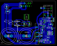
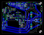
Still working it out.
Ok, well here is how it it is coming together now. I was having a rough time routing the GND path for the protection circuit, so I used a copper flood but only for that section. If it does not seem good, then I will work to fix that. Otherwise.... well any input is valued.
Ok, well here is how it it is coming together now. I was having a rough time routing the GND path for the protection circuit, so I used a copper flood but only for that section. If it does not seem good, then I will work to fix that. Otherwise.... well any input is valued.
Attachments
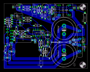
UnixMan said:Mauro, Russ:
what about a full ground plane on the other side?
I thought about that, but I think Mauro seems to recomend a more "organized" gounding approach.
Also, I really want to keep the design single sided, like the original.
Not a bad suggestion though.
Hi Paolo.
I have recommended the use of ground planes separate ( independently from the layer ) because the power sections manage currents in degree of modulates any "virtual ground " and then insert of the errors in the nets of NFB.
In practice I uses was technical of separation used in the A/D and video circuits.
In the digital electronics ( and RF ) is a lot of diffused the practice of the " multi-layer power planes " because is a lot of effective in the "shielding". In audio the "shielding" is less important, but it is a lot of more important the "stability" of the "virtual gnd "...
Naturally this work is a synthesis of compromises...
Ciao
Mauro

How to positioning " to zones " are.
I would connect the GND of the Relay control to the track of power gnd of the Relay contact, to avoid that it current with the relay influences the node ( jumper ) that feeds the signal GND.
After are able strengthens the power track and the signal GND.
If want have wander to line up some component and increase the distance among the pads (isolation)...
Ciao
Mauro
mauropenasa said:How to positioning " to zones " are.
I would connect the GND of the Relay control to the track of power gnd of the Relay contact, to avoid that it current with the relay influences the node ( jumper ) that feeds the signal GND.
After are able strengthens the power track and the signal GND.
If want have wander to line up some component and increase the distance among the pads (isolation)...
Ciao
Mauro
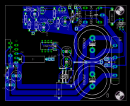
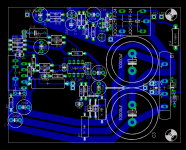
Thanks Mauro!
I was wondering about my signal GND being used for the speaker protection circuit.
Is this better?
Attachments
- Home
- Amplifiers
- Chip Amps
- My "audiophile" LM3886 approach