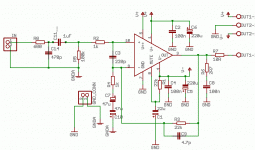
Okay, so this is my best pcb so far.
There is one pseudo ground star in it but I think it was not necessary as there are no large currents flowing (speaker ground returns to main capacitors).
I also left some space around the chip itself to allow more ways of mounting it to a heatsink.
There is of course an inductor wound around R7.
Signal and power grounds can be separated by shorting or removing the gnd_conn jumper.
Or it could be replaced with a 10ohm resistor (ground lifting iirc).
Btw, LM3886 GND pin belongs to signal or power ground?
Any ideas and suggestions welcome.
Attachments
Earlier version of the same thing:
http://www.diyaudio.com/forums/attachment.php?s=&postid=532242&stamp=1102964769
This one is much simpler and (probably) less stable. But anyway.
http://www.diyaudio.com/forums/attachment.php?s=&postid=532242&stamp=1102964769
This one is much simpler and (probably) less stable. But anyway.
breez said:I'm new to diy amplifiers, but 10 ohm in series at the output?
As mentioned, there is (not shown) an inductor that effectively shorts the resistor out at low frequencies
It's pretty good. 
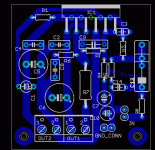
C10 is unnecessary. C7 is enough but it doesn't matter if you have C10 also.
C9 is also probably not so important and it have to be "tuned" for really compensate the input capacitance, which is the purpose of it.
I'm not totally happy about your long ground trace and C2, C4 at the end. Somehow I have tjhose caps be "closer" the LM chip. It's probably nothing to worry about but in this sense I like the BrianGT's board more (and mine also of course") ).
).
We have both doublesided boards so this make things more optimal, I know.
C10 is unnecessary. C7 is enough but it doesn't matter if you have C10 also.
C9 is also probably not so important and it have to be "tuned" for really compensate the input capacitance, which is the purpose of it.
I'm not totally happy about your long ground trace and C2, C4 at the end. Somehow I have tjhose caps be "closer" the LM chip. It's probably nothing to worry about but in this sense I like the BrianGT's board more (and mine also of course
).We have both doublesided boards so this make things more optimal, I know.
i agree with P-A,the ground trace is not too good.
FYI:
here is my non-inverted LM3886 layout,
http://www.diyaudio.com/forums/showthread.php?postid=541399#post541399
sch file,
http://www.diyaudio.com/forums/showthread.php?postid=499078#post499078
zang
FYI:
here is my non-inverted LM3886 layout,
http://www.diyaudio.com/forums/showthread.php?postid=541399#post541399
sch file,
http://www.diyaudio.com/forums/showthread.php?postid=499078#post499078
zang
peranders said:It's pretty good.
Thanks
While they are not essential, they surely won't hurt anyone. And all of the mentioned components could be simply left out.C10 is unnecessary. C7 is enough but it doesn't matter if you have C10 also.
C9 is also probably not so important and it have to be "tuned" for really compensate the input capacitance, which is the purpose of it.
We have both doublesided boards so this make things more optimal, I know.
Exactly. Unfortunately, making double sided PCBs is very difficult with my tools and skills.
Thank you both for your input.
Doublesided pcb with only ground plane is quite easy.
When you etch, put tape, any kind but wide tape is the best at the groundplane side, the solderside in your case I think, easier. Etch the board. After ecthing, remove the tape and drill the holes which shall not be in the groundplane. See my picture
An externally hosted image should be here but it was not working when we last tested it.
When you etch, put tape, any kind but wide tape is the best at the groundplane side, the solderside in your case I think, easier. Etch the board. After ecthing, remove the tape and drill the holes which shall not be in the groundplane. See my picture
peranders said:Doublesided pcb with only ground plane is quite easy.
When you etch, put tape, any kind but wide tape is the best at the groundplane side, the solderside in your case I think, easier. Etch the board. After ecthing, remove the tape and drill the holes which shall not be in the groundplane. See my picture
This idea is simply brilliant!
So it's like having a huge ground plane of very small resistance that virtually cannot form any ground loops? I'll surely try that out.
Re: Ground Plain
I have used "Electrolube DCA SCC3 Conformal coating", type DCA200H lately and some other type before.
It's a good idea to have some coating!
My handmade pcb's have protective coating, also in the picture above. It's an advantage if you can solder through it!kkchunghk said:Hi peranders,
I have also thought about making the top PCB side the ground plain. Would it be good practice to seal the surface with paint? Any brand with a funky colour you can recommend?
Cheers,
KK
I have used "Electrolube DCA SCC3 Conformal coating", type DCA200H lately and some other type before.
It's a good idea to have some coating!
Where do you have the speaker ground now?wxn said:How about this one?
LM3886 prototype finished
So in the end I decided to do it all without pcb. P2P is simply beautiful when done correctly.
One channel (of four) finished, very compact, no hum or oscillation, 6mV DC offset. PSU done p2p too. Pictures coming soon
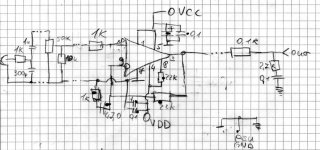
Anyway, for the final stage of assembly, just want to make sure I won't make a stupid mistake or smth. I attached the schematic, sorry for the quality, I'm a bad drawer. The central part is tightly packed on the chip itself, the dots mean a peace of wire. Btw, those electrolytics are 100uF, there are 10000uF caps per rail in the PSU (snubberized of course )
Parts marked with a dark dot are mounted and tested, the rest waiting to be soldered.
Any errors/comments? Btw, that 0.1R resistor should be near the chip or the output jack?
So in the end I decided to do it all without pcb. P2P is simply beautiful when done correctly.
One channel (of four) finished, very compact, no hum or oscillation, 6mV DC offset. PSU done p2p too. Pictures coming soon
Anyway, for the final stage of assembly, just want to make sure I won't make a stupid mistake or smth. I attached the schematic, sorry for the quality, I'm a bad drawer. The central part is tightly packed on the chip itself, the dots mean a peace of wire. Btw, those electrolytics are 100uF, there are 10000uF caps per rail in the PSU (snubberized of course
)Parts marked with a dark dot are mounted and tested, the rest waiting to be soldered.
Any errors/comments? Btw, that 0.1R resistor should be near the chip or the output jack?
Attachments
hi, wxn
You hand my little experience:
C7 has to be at least of 150 µF to guarantee you a good THD under the 100 Hz ( otherwise increases of about 10-20 times in comparison with 1Khz ).
How to absolute rule, you put the net of zobel (R6 C8) on the GND that uses for the loudspeakers, and separates the GND of power from that of signal ( as your first circuit ).
Colleague the 3 GNDS (GNDAP+GNDPW+GND_SIG) to the star center of the electrolytic cap. with 3 separate lines. Other suggestion, improves the common mode rejection way putting 100nF 100V among V+ and V-, near to R1. This technique performs miracles without create Feedback GND problem (all present on standard +- Bypass power)
Ciao
Mauro
Yes, I am aware of this ground-separation thing. I will definitely return speaker gnd/zobel to main capacitors but as for signal ground, I did it the "bad" way and had no problems - so why bother? I mean, this is supposed to be a pretty project, not technically perfect. Maybe next time when I have a proper pcb etc...
Btw, what did You have in mind by saying "near to R1"? Simply as close to the chip as possible?
Btw, what did You have in mind by saying "near to R1"? Simply as close to the chip as possible?
Yes, Simply as close to the chip as possible.
About GND "bad" or not, my suggestions are general.
If applies them, will work you always all at the first attempt, otherwise some circuits will go well to other no.
After to this things is the difference among a widens excellent and a cheap. If they be wrong the points of connection of the GND of power for example, you are able distort after 0, 02 % typical of this chips fine 0,2 %. If have not tool, with this rules six sure.
Good work
Mauro
- Status
- This old topic is closed. If you want to reopen this topic, contact a moderator using the "Report Post" button.
- Home
- Amplifiers
- Chip Amps
- LM3886 pcb approval wanted