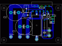
How does it look? It's an IGC, I plan on soldering the NFB resistor directly to the chip. Should I connect the grounds together on board like this?
Also, does anyone know of any good (read cheap) boardhouses in canada? A walkthrough of how to order boards would also be nice, like what files I need to send them, how to make said files, etc.
Also, does anyone know of any good (read cheap) boardhouses in canada? A walkthrough of how to order boards would also be nice, like what files I need to send them, how to make said files, etc.
") .
.As it is, the signal ground and power ground meet at the ground pin, no power current will go through the signal ground, so in effect it is star grounded. Yes?
What's wrong with the signal path? Too close to the output? How should I change it? Note the "IN1" is the signal ground and the loop is meant as a guard trace.
Thanks Upupa Epops, I will give the output resistor a little space.
What's wrong with the signal path? Too close to the output? How should I change it? Note the "IN1" is the signal ground and the loop is meant as a guard trace.
Thanks Upupa Epops, I will give the output resistor a little space.
I'm starting to try to learn this PCB stuff too. It would be nice if they had a whole separate forum devoted to the subject dealing with theory...software...PCB houses...etc.
I'm laying out a LM4782 3-channel PCB...but it's non-inverted. I'm using the schematic at the end of the data sheet. I looked at the "LM4782 inverted schematic" to get the gist of "inverted" layouts. Although, yours is different.
Anyway, assuming your schematic is correct...and in my ignorance...why wouldn't you do the following:
As the trace comes out the bottom of resistor #1 then immediately take it straight "west" to meet up with ground.
Also, leave the trace coming out the "west side" of IN1 (signal ground)...so it meets up with ground.
Then get rid of everything on the east side of IN1 including that part the comes down from resistor #1 and the part that loops around...I believe you refered to is as a "guard trace".
Maybe you can explain to me what a guard trace is.
Please, forgive this noobe...
By the way, I've done a lot of Googling to try an find a good deal on PCB fabrication.
It seems like www.PCBFabExpress.com has the best deal by far. Anything up to a 20 square inch board goes for 13 USD (minimum order of 5 boards). That includes 2oz. copper double sided, both side solder mask, and silk screen printing on the top side. They also have a "barebone" option. You have to do the math to see what is the better deal.
This company has a rather interesting concept. They are essentially aggregators. Their engineers work out of their homes. They take individual orders and "panel them up" into large panels. Then they contract with a number of fabricators (in silicon valley with ISO-9002 certification) to make the boards. Then, they have their own on-site employees do a quality check before shipping the finished boards out to the customer.
With the telecom and internet bust, I think the PCB industry became oversaturated, especially in Silicon Valley. These guys have figured out a "middleman niche" to leverage that excess capacity.
They've made it so that the big production outfits don't have to deal with a bunch of little orders. In fact their engineers don't have to be involved at all. They're just getting full gerber files for doing full large panels. The last step being routing out all the small boards. Then the on-site employees take the boards from there.
So PCBFabExpress doesn't have any capital tied up in plant or equipment. If one fabricator messes up...there are dozens of others across Silicon Valley needing to fill up excess capacity.
The only gotcha in using their service is that you must provide them with Gerber 274X files for your PCB. This has become the "generic format".
Tim_X...it looks like you are using some kind of layout software. What software are you using? Maybe it will output this format.
If not, I may have a recommendation as to some good software that does ($50 USD).
I have never had any boards fabed yet. Maybe someone has delt with these people.
Anyway...I've droned on long enough...
...Good luck on your project...
captain said:
It seems like www.PCBFabExpress.com has the best deal by far. Anything up to a 20 square inch board goes for 13 USD (minimum order of 5 boards). That includes 2oz. copper double sided, both side solder mask, and silk screen printing on the top side. They also have a "barebone" option. You have to do the math to see what is the better deal.
Olimex (www.olimex.com) has boards for about $25 bucks with only one piece. And they take eagle files, so you can get eagle for free and have the boards made by them.
carlmart said:The signal ground path should be re-arranged and not connected as you did.
Tim, this is good advice.
Power ground should stop on the film bypass caps, C3 and ? (reference not clear).
I'm using Eagle, it's freeware.
The guard trace just provides some extra isolation from the other traces on board, it's not really needed, but their was no reason not to so...
What's wrong with my signal path? Carlmart? Carlosfm?
It's C6, and I don't agree with you here, the purpose of the bypass caps is to keep the supply pins low impedance at high frequencys, so they should be connected as close as possible to the IC pins.
Or are you saying pin 7 should only connect to signal ground?
The guard trace just provides some extra isolation from the other traces on board, it's not really needed, but their was no reason not to so...
What's wrong with my signal path? Carlmart? Carlosfm?
Power ground should stop on the film bypass caps, C3 and ? (reference not clear).
It's C6, and I don't agree with you here, the purpose of the bypass caps is to keep the supply pins low impedance at high frequencys, so they should be connected as close as possible to the IC pins.
Or are you saying pin 7 should only connect to signal ground?
Tim__x said:Or are you saying pin 7 should only connect to signal ground?
That's what I'm saying.
You sould join signal and power grounds at the board bottom, and not on the chip.
Use a small value resistor, like 1~2.2ohms to join signal and power grounds.
- Status
- This old topic is closed. If you want to reopen this topic, contact a moderator using the "Report Post" button.
- Home
- Amplifiers
- Chip Amps
- Yet another LM3886 PCB