Greetings from Finland
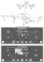
I have been designing a little board to LM3886 audio amplifier IC. I have used SMD components to minimise board area and signal length. Board size is 80mm X 32mm, mainly because large capacitors.
This is inverting version but the non inverting is also coming at same board size of course. Some component reliefs have to be done before first proto PCBs but maybe some two weeks and first proto is ready to be tested.
Some comments please.
Attachments
Check the valure of the input cap once more, way too small. You will get a bass cut at 159 Hz! 10-47 uF is more appropiate.
C2, very thin ground connection and also in the wrong place. Try to get the power ground as compact as possible. Why don't you do like I have done? I have the power at the left and the signal at the right.
C2, very thin ground connection and also in the wrong place. Try to get the power ground as compact as possible. Why don't you do like I have done? I have the power at the left and the signal at the right.
An externally hosted image should be here but it was not working when we last tested it.
Yes the C3 value is definetly too small, didn't calculate that value, I just put it there, hmm.. maybe careless designing.
I don't know what you are meaning, is C2 in wrong place or ground???
That thin ground is not affecting ground potential or anyway it does not carry large currents . Main ground is deployd from those wire holes.
I don't know what you are meaning, is C2 in wrong place or ground???
That thin ground is not affecting ground potential or anyway it does not carry large currents . Main ground is deployd from those wire holes.
Sorry, I didn't see it clearly. Your grounding seems to be Ok.
The difference between your and mine design is that I have chosen to have low values for the feedback and this forces me to use a buffer and since I don't want any eletrolytic caps in the signal path I have chosen to have a DC-servo instead.
With a non-inverting buffert any signal source can be connected. If you have 10 komhs in your case you might have trouble to connect a potentiometer and if this potentiometer has too high resistance it will effect on gain and feedback of the LM3886. I'm not sure if you can bump into stability problems (gains less than 10). Otherwise a good layout. You have put the signal ground very close to speaker ground, that good and if you want to make it perfect, draw and insulated trace to the speaker ground pad. If you do that you avoid any voltage drops caused by currents to and from the C1.
You might manage without any output filters but if you have a difficult load it may not be good to omit the filters.
....yeees...., but these may also be essential in some applications in oder to achieve good sound reproduction which has to do with a stable amp. These filters are for frequency compensation of the output stage (which may not be obvious) and also some protection for incoming RFI.JJJ said:If you want to draw a simple small board something must be left out, and those output filters were mayby first ones.
I don't know how you are going to make the boards but I think it's smarter to have those filter on board and start not to use them. It's very easy to add these filters if you experience problems.
JJJ said:I looked up that input capacitor and i have forgot input resistor from capacitor end to ground. With capacitor value 1uF and resistor value 10K, Low Fs would be about 16Hz.
If you mean that the amp side of the cap gets a resistor to ground then that will not make the Fs lower but higher since it will be in parallell with the previous determining impedance AFAIK.
- Status
- This old topic is closed. If you want to reopen this topic, contact a moderator using the "Report Post" button.
- Home
- Amplifiers
- Chip Amps
- Upcoming LM3886 SMD board