Hello everyone who is interested!")
By looking through the forum for a month or so, I found a lot of interesting GC projects. Since, I'm about to build my own GC, based on the National's LM3886, I decided to make a PCB for it. I have to thank to BrianGT and Peter Daniel, because I was mostly inspired by their great LM3875 GC PCB set , and I should not forget mentioning great work of digi01
My project would, probably, contain a regulated PSU (one per channel) and most probable I'll try to make LM4780 bridged/parralel PCB to drive my sub. The reason why I started that thread is rather simple - I just want to try something like that myself and I'm shure I'll need assistance
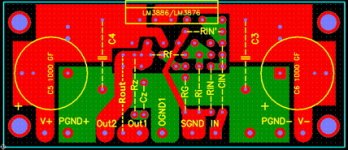
The PCB provide the possibility to use it for the inverted or non-inverted amplifier. There also included the possibility to play with T-network feedback solution. There is no specific schematic used for this project, but as for the reference one can use National's AN-1192 application note (see page 6). You have to assume using only one part of the schematic there (either top or bottom). I've tried to make it universal, that I can play with the different configurations later. Zobel network and power cap bypassing is provided too (just in case ... ). But I do not provide the space for the most of other capasitors...
The picture of the board is in the attachment.
The size of the board is 31.5 mm x 74 mm (1.24" x 2.91") and the grid you see there is 1 mm or 39 mills.
Any suggestions and ideas are welcomed
By looking through the forum for a month or so, I found a lot of interesting GC projects. Since, I'm about to build my own GC, based on the National's LM3886, I decided to make a PCB for it. I have to thank to BrianGT and Peter Daniel, because I was mostly inspired by their great LM3875 GC PCB set
, and I should not forget mentioning great work of digi01 My project would, probably, contain a regulated PSU (one per channel) and most probable I'll try to make LM4780 bridged/parralel PCB to drive my sub. The reason why I started that thread is rather simple - I just want to try something like that myself and I'm shure I'll need assistance
The PCB provide the possibility to use it for the inverted or non-inverted amplifier. There also included the possibility to play with T-network feedback solution. There is no specific schematic used for this project, but as for the reference one can use National's AN-1192 application note (see page 6). You have to assume using only one part of the schematic there (either top or bottom). I've tried to make it universal, that I can play with the different configurations later. Zobel network and power cap bypassing is provided too (just in case ...
). But I do not provide the space for the most of other capasitors...The picture of the board is in the attachment.
The size of the board is 31.5 mm x 74 mm (1.24" x 2.91") and the grid you see there is 1 mm or 39 mills.
Any suggestions and ideas are welcomed
Attachments
Hi Vasja
Really nice layout. I also like the fact that you incorporated the possibilities to use a T-network and/or a Zobel. I myself have been playing with the idea of a PCB that has it all. The amp itself, ofcoarse, the T-network, the Zobel and a buffer. Sofar this has never been done. And then I even don't mention a regulated PS! Maybe an idea for you? The first "GC board that has it all".
Cheers
Walter
The main bypass capacitors are too far away from their respective pins, and the only reason to use a double sided pcb is to join the power ground pins.
Put the caps on the left, as close to pins as you can, and use single sided pcb.
Also provide option to use smaller eletrolytic cap even closer to pins when using regulators. Additional bypass can go on copper side, directly over pins, with SMD parts.
I can't find the bypass cap for mute pin, as data sheet suggests.
Carlos
To GeWa:
Thanks for good words
I'm currently thinking about making all the things you mentioned, but it will take time
To carlmart:
If I understood correctly, you suggest me to place big caps in the way like digi01 used in his design ... Concerning bypass caps, I can move them closer to the pins of the chip, but than I would have to use smaller caps, which is usually not a good idea.
And you may probably noticed, that in case if bypass caps are eliminated one can turn big electrolitic caps towards the chip. I've also eliminated the bypass cap for mute pin, as most people doing, but I will try to provide the room for it.
But all these problems occure just because I'm trying to make a universal PCB and a lot should be probably done in order to adjust it for better performance. And thank you for suggestions, I'll try to work on them
Just wondering what is RG? Pretty good effort but it seems you have copied Brain's error too, the grounding. Signal ground should be connected directly to the pad OG. Signal ground should"sniff" the speaker ground. If yoiu do so you will avoid voltage drops from the smotthing caps which leads to increased distortion, not much though but you will get more than the LM3886 itself produces. You will get 0.02% or so more dist. It's just an estimation.
The decoupling caps will probably work where they are but I would suggest 100 nF/63 V polyester, 2.5 x 5 mm caps closer to the pins of the LM3886.
BTW: It's pretty easy to patch Brian's pcb for 100% correct grounding. Note also that this isn't a serious error. The LM4780 pcb from Brian is 100% correct in this sense.
The RG is the resistor from the signal ground to the power ground. I've seen ones such a design, where insted of simple wire connection between signal and power ground points the small value resistor was used.
And I forgot to mention I have not too much of experience with PCB design (and in building of amplifiers as well) I really need help from professionals. And I have to revisit Brian's LM4780 PCB project for ground layout
And I forgot to mention I have not too much of experience with PCB design (and in building of amplifiers as well)
I really need help from professionals. And I have to revisit Brian's LM4780 PCB project for ground layout 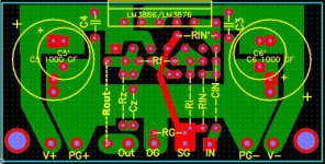
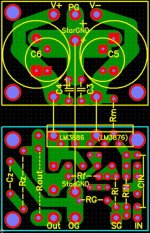
By thinking on what was suggested in the replies I decided to make another kind of layout. It consists of two boards of equal size 1.34" x 0.95", which should be mounted bottom-to-bottom and the pads linked with the yellow trace should be connected with the thick wire. The distance between two boards is about 5 to 10 mm and mostly depends on how long are the leads left after soldering.
The only problem I can see here is the fact, that the negative PS rail will go just beneath the input area. Most probably I would have to introduce the ground plane on the caps board.
... and I still have to think where to put 8 rectifiers
The boards are in the attachment...
The only problem I can see here is the fact, that the negative PS rail will go just beneath the input area. Most probably I would have to introduce the ground plane on the caps board.
... and I still have to think where to put 8 rectifiers
The boards are in the attachment...
Attachments
- Status
- This old topic is closed. If you want to reopen this topic, contact a moderator using the "Report Post" button.
- Home
- Amplifiers
- Chip Amps
- LM3886 PCB project and may be more