Hi All-
I am working on another LM3886 PCB but this PCB needs to be as narrow as possible. I am hoping to make the PCB just slightly wider than the actual chip. I will be using "smallish" caps on the PCB and additional caps on the pwr supply board. Also components on both sides as needed to help minimize the size.
What I am requesting in this thread (so we can kill it quickly) is for someone's file from ExpressPCB or Eagle that I can use for the LM3886 mounting holes.
They are NOT the standard .100 spacing, and I am not having any luck making my own from scratch.
Any assistance would be appreciated.
Thank you in advance,
Troy
Edit: Email address might be nice... stgrab@yahoo.com
rabstg said:Hey Carlos-
Library file for Eagle.
Sorry, not an Eagle user.
Carlos
narrow 3886 PCB
Check here http://www.diyaudio.com/forums/showthread.php?s=&threadid=40680, in particular my posts 8-10 where the actual files are.
Rodolfo
Check here http://www.diyaudio.com/forums/showthread.php?s=&threadid=40680, in particular my posts 8-10 where the actual files are.
Rodolfo

Sorry if I was confusing Rabstg.
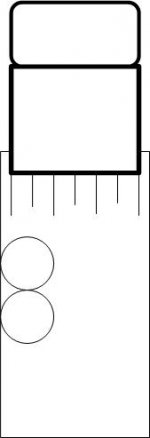
Placing the IC across the PCB end as per your sketch, determines the minimum board width at the distance between opposite extreme pins (0.66" / 17.76 mm) plus hole and pad allowances. Also, device width is 0.78" / 19.89 mm.
Placing the IC with the dual pin rows parallel to the PCB length imposes a minimum width of 0.19" / 4.83 mm plus hole and pad allowances. This is as narrow as it could be made but not practical, for components should be spread at the sides and routed with narrow traces. Yet you see there is a margin to use for increasing board width yet keeping below 1/2". The added benefit is you may place several devices on the same board.
Hope this helps.
Rodolfo
All right. I spent the last 34 hours trying to draw a PCB in Eagle and have stopped before I break something. Most likely my brain.
I will attach the crappy Eagle file I'm got too if anyone is bored.
Thanks.
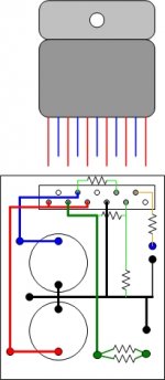
Well I am trying draw a PCB like this:
I will attach the crappy Eagle file I'm got too if anyone is bored.
Thanks.
Well I am trying draw a PCB like this:
Attachments
Didn't you see the Yarg?
Hi rabstg,
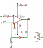
I'll post my current workfiles of my LM3876/86 project called Yarg, in case you still plan on doing something with the LM3886.
I'm progressing slowly too at the moment, as lectures just start again after the summer break.
Hint: please don't use the auto router to do anything meaninful regarding an Eagle layout. I consider the auto router usefull for just one thing: testing wether your placement allows passing all signals along. Once I've confirmed that my component placement requires minimal or no signal crossing, I start doing the actual signal routing by hand (wire by wire) individually, using different widths and polygons where neccessary. The Cadsoft PDF documentation and tutorial help a lot here...
What prevents your design from advancing is the fact that you are hiding the pin connections in the schematic. In the schematic editor, just type the command 'display' followed by [enter]. This will bring up a dialog window (see the now selected button in the toolbar to find that dialog via mouse again) that lets you select the visible schematic 'layers' (circuit aspects, in other words).
In your schematic, layer 93 (pins) is hidden (please unhide it). That's why you couldn't safely connect RMUTE and pin 8 of the LM3886 (the circles around the component pins are the place where a wire connection 'snaps' in and sits). And that's why you can't route this wire on the board (eagle prevents you from doing that as long as the signal connection is not defined in the schematic).
You can always either place the components with the pin 'circles' joining (and then move them apart to pull a wire inbetween) or place them next to each other and use the 'wire' command to actually draw the wire from one pin 'circle' to the other. The former method is quicker, the latter is better style...
When you open my schematic, don't let the high number of components fool you, just use a copy of the file to reduce the schematic to what you want.
When you open the board, first enter the command 'ratsnest' followed by [enter] in order to have all polygon wires rendered beautifully. You'll notice that nearly everything is SMT, but you can use the command 'change technology' to replace the device style of resistors and capacitors by whatever you like...")
Hope this helps,
Sebastian.
Hi rabstg,
I'll post my current workfiles of my LM3876/86 project called Yarg, in case you still plan on doing something with the LM3886.
I'm progressing slowly too at the moment, as lectures just start again after the summer break.
Hint: please don't use the auto router to do anything meaninful regarding an Eagle layout. I consider the auto router usefull for just one thing: testing wether your placement allows passing all signals along. Once I've confirmed that my component placement requires minimal or no signal crossing, I start doing the actual signal routing by hand (wire by wire) individually, using different widths and polygons where neccessary. The Cadsoft PDF documentation and tutorial help a lot here...
What prevents your design from advancing is the fact that you are hiding the pin connections in the schematic. In the schematic editor, just type the command 'display' followed by [enter]. This will bring up a dialog window (see the now selected button in the toolbar to find that dialog via mouse again) that lets you select the visible schematic 'layers' (circuit aspects, in other words).
In your schematic, layer 93 (pins) is hidden (please unhide it). That's why you couldn't safely connect RMUTE and pin 8 of the LM3886 (the circles around the component pins are the place where a wire connection 'snaps' in and sits). And that's why you can't route this wire on the board (eagle prevents you from doing that as long as the signal connection is not defined in the schematic).
You can always either place the components with the pin 'circles' joining (and then move them apart to pull a wire inbetween) or place them next to each other and use the 'wire' command to actually draw the wire from one pin 'circle' to the other. The former method is quicker, the latter is better style...
When you open my schematic, don't let the high number of components fool you, just use a copy of the file to reduce the schematic to what you want.
When you open the board, first enter the command 'ratsnest' followed by [enter] in order to have all polygon wires rendered beautifully. You'll notice that nearly everything is SMT, but you can use the command 'change technology' to replace the device style of resistors and capacitors by whatever you like...
Hope this helps,
Sebastian.
Attachments
- Status
- This old topic is closed. If you want to reopen this topic, contact a moderator using the "Report Post" button.
- Home
- Amplifiers
- Chip Amps
- Another LM3886 PCB!!