Hello,
I'm planning to make a chipamp of my own that uses TDA7294. I have planned to split signal and power supplies, with signal supply a little bit higher than power one.
I've juste run through some threads about TDA729x. Some were talking about bad (smoky) experiences with splitting supplies of signal/power stages.
Finally, did someone have it work?
Seeya.
Hallo,
As far as i can see, split supply is meant to raise the efficence of power consumption in the original datasheet, not to improve sound quality, and i guess, that's what you intend.
If you like, have a look on this kit using the 7293, but use of 7294 with the newer pinout is possible too.
Complete kit in 'high-end' version is about 50 euros, 40 in standard version. Naked pcb's are also available.
Ulrich Böhmke worked on this boards for several years, and its probably very well-engineered.
http://www.schuro.de/preisl-amp80.htm
Sorry, its only in german, but the schematic may help anyway.
Here it is with a short handbook in english.
http://www.ub-elektronik.de/downloads/a80-short.pdf
Andreas
I intend 2-3 things:
- a cleaner signal supply, since TDA's PSRR is not so good
- not too much heating due to overvoltage on power supply
- avoid undervoltage and therefore clipping of signal part on highly demanding transients: I plan to have a voltage a bit higher on signal supply vs. power supply.
Anyway, having your answer on my topic makes me feel less alone on this subject
Hi,
its clear, that the TDA family of Audio-IC's is somehow understimated in this forum, cause all seem to go for National Semiconductor LM's.
But Where did you get that from:
'clipping of signal part on highly demanding transients. I plan to have a voltage a bit higher on signal supply vs. power supply.'
I think SGS-Thomson did theire jobs as well, and there's no need to worry about.
Andreas
PS: i'ld like to discuss more TDA 72XX issues.
Hello Shongi,
On TDA7294 datasheet, THD at 1kHz for 27V supply and 4R load increases badly at about 60W, which I take as clipping. By looking at the simplified schematic of TDA, I presume that signal part clips before power part.
I'm working on a 5 channel amplifier. I've made some simulations of my transfo + power supply + bypass caps + emulation of 30Hz high amplitude transients into 4 ohm load on all channels.
Of course, this provokes a temporary drop-out of supply voltage. This makes my supply rails go down to 25.5V worst case.
From that, I had 3 solutions to stay away the most possible from clipping in this situation:
- share signal/power supply and that's all folks => hum, can't I try something better?")
- share signal/power supply and raise it to get the last watts => it's overkill, without even talking about heat sinking (remember: it's a 5 channel amplifier), noise on signal supply, etc.
- split signal/power supply, and keep signal supply >= power supply => yeah, that's a try worth the game
In my worst case, whereas my power supply gets as low as 25.5V, my signal supply only drops to 28.5V.
Ok, I made a number of assumptions that needs testing. I'm nearly ready to do those tests , maybe next week-end

On TDA7294 datasheet, THD at 1kHz for 27V supply and 4R load increases badly at about 60W, which I take as clipping. By looking at the simplified schematic of TDA, I presume that signal part clips before power part.
I'm working on a 5 channel amplifier. I've made some simulations of my transfo + power supply + bypass caps + emulation of 30Hz high amplitude transients into 4 ohm load on all channels.
Of course, this provokes a temporary drop-out of supply voltage. This makes my supply rails go down to 25.5V worst case.
From that, I had 3 solutions to stay away the most possible from clipping in this situation:
- share signal/power supply and that's all folks => hum, can't I try something better?
- share signal/power supply and raise it to get the last watts => it's overkill, without even talking about heat sinking (remember: it's a 5 channel amplifier), noise on signal supply, etc.
- split signal/power supply, and keep signal supply >= power supply => yeah, that's a try worth the game
In my worst case, whereas my power supply gets as low as 25.5V, my signal supply only drops to 28.5V.
Ok, I made a number of assumptions that needs testing. I'm nearly ready to do those tests , maybe next week-end
Here is one of the tests I made:
+15V --[22R]--> to TDA positive signal supply and bypass caps (100uF//150nF)
Same on negative signal supply
+15V --[22R]--> to TDA positive power supply and bypass caps (10.000uF//100nF)
Same on negative power supply
Here is what I got, when TDA is not on stand-by:
- 8mA on SVss, 4mA on SVdd
- 40mA on PWVss, same on PWVdd
The voltage drop from signal to power supplies was therefore about 22*(40mA-8mA) = 0.7V
No problem encountered here...
This confirms a thing of "high efficiency" application note: having signal supply higher than power supply is not a problem, at least if power part does not clip.
From what I read on DIYaudio, it's signal supply being below power supply that causes problems.
- TDA can be fed with separate power supplies, provided than +Vs >= +PWVs, and most important of all -Vs <= -PWVs.
The datasheet indicates than -Vs is connected to the metal tab, which indicates that the substrate who sets the reference potential for the chip is -Vs. If the chip experiences a potential lower than -Vs, then the substrate will be reverse-biaised and be damaged!
- the above double-supply issue stays the same even if TDA is on stand-by
- seems like mute/stand-by pins act almost directly on transconductance stage. They are suceptible to noise picking, and should be referenced to signal ground!
I've blown up 2 chips (and many brain cells) on the topic... Designing a double supply where power supply never exceeds signal supply is not a big trouble (no load, max load). Ensuring the same property when supply starts, or when switching stand-by is not very difficult too.
the BIG trouble is to ensure that power supply does not exceed signal supply during "power down" transient.
Here are the only solutions I found:
1) having TDA's bypass caps discharge into signal supply when powering down. That is, inserting a diode between PWVs and Vs. In order to keep PWVs <= Vs, it means inserting another diode between bypass caps and TDA. It's the solution described in TDA7293 datasheet. The 2 diodes between power supply bypass caps and TDA must support TDA max current (~6.5A). Moreover, the couple of diodes may add "high frequency" noise, and distorsion: power diode switched on/off when TDA working in class B, and power diode I/V characteristic is not linear but logarithmic.
2) same idea, but using FETs driven by amplifier state instead of junction diodes. Costly, similar nois/distorsion issues (Rds on does non negligible when operating at high power in class B), may require additional heat sinking.
3) adding a discharge circuit to discharge bypass caps when amplifier is switched off. For a 5 channels amplifier with 80mF on the power supply side vs 1.5mF on the signal supply side, it means more than 30W to dissipate for 30 seconds! And any fault in the discharge circuit means that all TDAs will burn out
4) having a regulated power supply controlled by amplifier state, only small bypass caps near the TDA, and a resistor bypassing these small bypass caps .
I don't like solutions 1) and 2). I don't have space and heatsinking left for solution 3), which is a bit risky IMHO.
Solution 4) does not fit well my 5 channels amplifier: path from supply to TDAs is too long (30 cms) for small bypass caps, IMHO. And it would imply a complete re-design of my supply.
My WAF and I think that I spent already too much time on these PSU issues, so I leave it, and go for single supply.
(single, but regulated )
The datasheet indicates than -Vs is connected to the metal tab, which indicates that the substrate who sets the reference potential for the chip is -Vs. If the chip experiences a potential lower than -Vs, then the substrate will be reverse-biaised and be damaged!
- the above double-supply issue stays the same even if TDA is on stand-by
- seems like mute/stand-by pins act almost directly on transconductance stage. They are suceptible to noise picking, and should be referenced to signal ground!
I've blown up 2 chips (and many brain cells) on the topic... Designing a double supply where power supply never exceeds signal supply is not a big trouble (no load, max load). Ensuring the same property when supply starts, or when switching stand-by is not very difficult too.
the BIG trouble is to ensure that power supply does not exceed signal supply during "power down" transient.
Here are the only solutions I found:
1) having TDA's bypass caps discharge into signal supply when powering down. That is, inserting a diode between PWVs and Vs. In order to keep PWVs <= Vs, it means inserting another diode between bypass caps and TDA. It's the solution described in TDA7293 datasheet. The 2 diodes between power supply bypass caps and TDA must support TDA max current (~6.5A). Moreover, the couple of diodes may add "high frequency" noise, and distorsion: power diode switched on/off when TDA working in class B, and power diode I/V characteristic is not linear but logarithmic.
2) same idea, but using FETs driven by amplifier state instead of junction diodes. Costly, similar nois/distorsion issues (Rds on does non negligible when operating at high power in class B), may require additional heat sinking.
3) adding a discharge circuit to discharge bypass caps when amplifier is switched off. For a 5 channels amplifier with 80mF on the power supply side vs 1.5mF on the signal supply side, it means more than 30W to dissipate for 30 seconds! And any fault in the discharge circuit means that all TDAs will burn out
4) having a regulated power supply controlled by amplifier state, only small bypass caps near the TDA, and a resistor bypassing these small bypass caps .
I don't like solutions 1) and 2). I don't have space and heatsinking left for solution 3), which is a bit risky IMHO.
Solution 4) does not fit well my 5 channels amplifier: path from supply to TDAs is too long (30 cms) for small bypass caps, IMHO. And it would imply a complete re-design of my supply.
My WAF and I think that I spent already too much time on these PSU issues, so I leave it, and go for single supply.
(single, but regulated
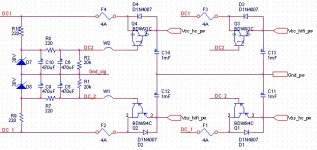
)Here is the regulator part of my single split supply.
It is derived from the power section of my previous dual supply. Since I have already made a prototype of the dual supply, I chose to modify it rather than making a new PCB and buying new components.
It is derived from the power section of my previous dual supply. Since I have already made a prototype of the dual supply, I chose to modify it rather than making a new PCB and buying new components.
Attachments
alim
Bonjour
donc une régulation linéaire
je vous avais posé la question car je suis en train d'étudier des enceintes 3 voies en filtrage actif donc 3 amplis par enceintes,
pour le moment je pense faire les essais avec une alim non régulée mais avec un filtrage en Pi par ampli : un condo de tête commun pour le secteur et filtrage en Pi pour chaque ampli.
La deuxième solution qui m'attire le plus étant une alim à découpage symétrique mais ce n'est pas courant et je ne suis pas décidé à la mettre au point.
David,
On aimerais bien que vous parliez Anglais ici.
We’d like you to speak English over here.
C’est peut-être dur pour vous mais la majorités des membres ne vous comprend probablement pas.
It might be a bit difficult for you but many members probably can’t understand what you want to tell them.
/Hugo
On aimerais bien que vous parliez Anglais ici.
We’d like you to speak English over here.
C’est peut-être dur pour vous mais la majorités des membres ne vous comprend probablement pas.
It might be a bit difficult for you but many members probably can’t understand what you want to tell them.
/Hugo
Re: alim
Not completely linear: zener does not conduct all the time, and BDW darlingtons have a base-to-emitter internal resistance on each transistor.
Initially, I had given some thoughts to switched mode power supplies, particularly H-bridge. Since I don't have any stuff to measure at HF, and since I don't have access to a SMPS transformators manufacturer, I gave up. Not talking about headaches inherent to HF routing :lol:
Concerning regulated (but non SMPS) PSUs, there was a nice regulated power supply using an IRF530 as a ballast (mated with a TL431 which acts as a comprator) about ten years ago in the french "LED" magazine (with the Freddy Mosfet Amp ).
About the TDA 7293, having heard both a Sakura gaincard and a Linn klimax Twin in the same system, it is clear for me that the TDA 7293 can do MUCH better than the Gaincard/Gainclones.
The major interest of chip amps is for me in the ability to match precisely transistors and control the bias in the output stage (i.e. great class AB current amplification stage). A very interesting application of the TDA 7293V could be in using it in slave only, together with an external, custom designed, voltage amplification stage.
I made some amps with tda 7295, and the sound is quite good; different to most, i use bigger caps, 4x4700uf, and as example: resolution cant be bad, when the difference between caps direkt on the wooden base and vibration reduced with some soft foam-rubber under the same caps is audible.
must say, first sound impression was disappointing, but step by step i found the better things;
must say, first sound impression was disappointing, but step by step i found the better things;
- Status
- This old topic is closed. If you want to reopen this topic, contact a moderator using the "Report Post" button.
- Home
- Amplifiers
- Chip Amps
- TDA729x split signal/power supplies