I want to bootstrap the LM3886 to run off +/- 75v rails.
The ground pin has to be 9v above the negative rail, but since the opamp's rails will be chaning with the signal, is it ok to connect the gnd pin to the output?
Where would the mute pin be connected? Would I connect it to the fixed supply negative rail?
What is common mode input voltage and differential input voltage?
are you designing for variable supply rails (like class-h) or rails that switch from 9volts to 70volts and back?
I'm not an expert with supply bootstraping for op amps, but my understanding is that you don't connect the output to ground. The mute pin would have to be connected to the -70volt supply rail. My understanding of common mode is when the signal connected to the non-inverting opamp input cancels with the signal connected to the inverting opamp input. My understanding of differential input is the difference in voltage between the non-inverting lead and the inverting lead of the opamp. Could someone confirm or correct me?
I'm not an expert with supply bootstraping for op amps, but my understanding is that you don't connect the output to ground. The mute pin would have to be connected to the -70volt supply rail. My understanding of common mode is when the signal connected to the non-inverting opamp input cancels with the signal connected to the inverting opamp input. My understanding of differential input is the difference in voltage between the non-inverting lead and the inverting lead of the opamp. Could someone confirm or correct me?
I'm designing for variable supply rails. But I thought that class H was switching between 2 different supply voltages.
As for the ground pin, after looking thru a document on bootstrapping and doing some simulations, I figured out that a voltage divider should work (resistor from v+ to gnd pin and resistor from v- to gnd pin). Can someone confirm this?
As for the ground pin, after looking thru a document on bootstrapping and doing some simulations, I figured out that a voltage divider should work (resistor from v+ to gnd pin and resistor from v- to gnd pin). Can someone confirm this?
Class-G is switching the supply rails to different voltages. Class-H is a variable supply rail voltage.
What are you trying to do with this voltage divider circuit? The ground pin on the lm3886 op amps should be kept at ground.
The voltage divider circuit created by rf and rg in the document you posted is used with the inverting input and it sets the gain of the opamp.
What are you trying to do with this voltage divider circuit? The ground pin on the lm3886 op amps should be kept at ground.
The voltage divider circuit created by rf and rg in the document you posted is used with the inverting input and it sets the gain of the opamp.
The LM3886 had undervoltage protection. The only way to disable it is to keep the gnd pin 9v above the negative rail. With varying rails, the negative rail (-37v) would be varying, and going close to 0v (simulations). Then the gnd pin would not be 9v above v-, and the undervoltage protection would shut off the chip.
With this voltage divider, I'm trying to keep the gnd pin voltage halfway between the varying rails.
With this voltage divider, I'm trying to keep the gnd pin voltage halfway between the varying rails.
xplod,
Your basic topology is sound, but a warning is in order. The way this is set up means a lot of extra (current) gain in the loop, also because you use a minimum (10x) gain overall. This is a strong invitation to instability, which will vary with the type of output transistors.
Also, the 100k input resistor (I can see where it comes from) just generates a lot of noise, and is unnessecary.
The resistor-diode string for the supply offset transistors is quite high impedance; remember that if the output swings toward a supply rail, the diodes still need enough current to be biased. Maybe a current source is better here.
In fact, if you want to use this topology, why use the LM3886? This is a power amp, and in this way, you just use it as a driver. There are good opamps that will give far better performance here and also avoid the instability problems.
Jan Didden
you use a minimum (10x) gain overall
Changed the gain to 25x.
Also, the 100k input resistor (I can see where it comes from) just generates a lot of noise, and is unnessecary.
Took that out.
The resistor-diode string for the supply offset transistors is quite high impedance; remember that if the output swings toward a supply rail, the diodes still need enough current to be biased. Maybe a current source is better here.
What do you mean by current source? (What is a current source?)
In fact, if you want to use this topology, why use the LM3886?
I have 20 of them (free samples--I was surprised that National sent me 4 packs of 5 of them in a row
") ) This will be used as part of a bridgeable sub amp, so performance doesn't matter that much. And it will be easier to do with the LM3886, because I can keep the rails at +/- 35v, instead of +/- 15 as with a regular opamp. (A regular opamp wouldn't swing to 75v, would it?)
) This will be used as part of a bridgeable sub amp, so performance doesn't matter that much. And it will be easier to do with the LM3886, because I can keep the rails at +/- 35v, instead of +/- 15 as with a regular opamp. (A regular opamp wouldn't swing to 75v, would it?)xplod1236 said:[snip]I have 20 of them (free samples--I was surprised that National sent me 4 packs of 5 of them in a row
You got me confused now. I thought you were going to bootstrap the LM's on +/- 60 (90?) volt supplies. That can be done with opamps also. If you want to use +/- 35V, does that mean you decided to junk the bootstrap scheme?
Jan Didden
I thought you were going to bootstrap the LM's on +/- 60 (90?) volt supplies.
I am.
If you want to use +/- 35V, does that mean you decided to junk the bootstrap scheme?
No. The 35v supplies are modulated with the output. At 0v output, the chip supplies will be +/- 35v. With the chip running, the positive supply will swing to +75v, and the negative will swing to 0v, and the other way around. The main supplies will be +/- 75v.
Sorry for the confusion.
Yes and no.
Yes:
I have 20 LM3886s and a 75v supply, and I want to build an amp. Now I would ask your question:
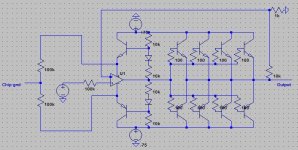
I already have a design (attached), and I'm looking for comments about it. I am using output transistors, because I want the amp to be bridgeable. Putting 150v (+75v and -75v) across the LM3886 is not a good idea.
Will this amp work? I did simulations of it, and it turns out ok. Does anyone see any problems with it? Which transistors should I use for the supply and output?
The writing on the schematic is small, so for those of you who can't read it, here it is (from left to right):
First is the input (signal generator), then an 80 hz low pass filter, then a phase splitter with a gain of 5x, and finally the amps (25x gain). The overall gain of the amp is 125x for single-ended, and 250x for bridged.
Yes:
I have 20 LM3886s and a 75v supply, and I want to build an amp. Now I would ask your question:
No:What is the best way to built an audio power amp, starting with a lot of LM3886'es and a +/- 75 V supply?
I already have a design (attached), and I'm looking for comments about it. I am using output transistors, because I want the amp to be bridgeable. Putting 150v (+75v and -75v) across the LM3886 is not a good idea.
Will this amp work? I did simulations of it, and it turns out ok. Does anyone see any problems with it? Which transistors should I use for the supply and output?
The writing on the schematic is small, so for those of you who can't read it, here it is (from left to right):
First is the input (signal generator), then an 80 hz low pass filter, then a phase splitter with a gain of 5x, and finally the amps (25x gain). The overall gain of the amp is 125x for single-ended, and 250x for bridged.
Attachments
xplod1236 said:
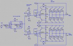
Be careful adding extra power transistors at the output. Because of the extra phase lag you are risking stability problems.
BTW, I am missing a proper bias set-up to get the output drivers in proper class AB. Now it will unnecessarily suffer from cross over distortion.
Cheers
I just realized that I don't need to bias the output transistors. The feedback is connected after the output transistors, and the opamp will compensate for the transistor bias. My simulation showed this as well.
This is from a document I found online. If anyone wants it, email me at xplod1236@wowway.com.
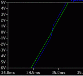
They even show graphs of the "jump", which looks exacly like my simulation (attached). The blue line is the opamp output, and the green line is the transistor output.
This is from a document I found online. If anyone wants it, email me at xplod1236@wowway.com.
The loss across the bias network and across the transistor have been compensated for by the op amp.
The crossover distortion is gone. During the crossover time, when both transistors try to turn off, the output of the op amp makes a jump of several volts to bias the opposite transistor on. So the flat spot in the output has been removed by the step in the op amp's output voltage.
They even show graphs of the "jump", which looks exacly like my simulation (attached). The blue line is the opamp output, and the green line is the transistor output.
Attachments
- Status
- This old topic is closed. If you want to reopen this topic, contact a moderator using the "Report Post" button.
- Home
- Amplifiers
- Chip Amps
- Bootstrapping LM3886