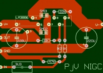
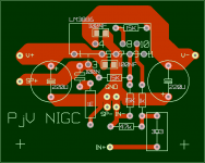
This is the pcb I have designed for the LM3886T device.
Before I have the pcb's done it would be nice if people that know a thing or two about pcb design could make some comments about this design.
Remarks:
- SMD1 & SMD2 are 100 nF caps, soldered to the bottom of the pcb.
- The hole for pin 3 of the LM is placed a little forward to make some room for the trace from Pin 1 to 5 to be wider.
- Rectifier & buffering is on a separate pcb.
Better not use an exact copy of pcb, the dimensions of the LM are wrong, as Layo doesn't have the multi-watt package.
(or maybe I just couldn't find it, after all it's my first try.
That might also explain why it took > 6 hours )
)
And for some reason if I scaled the file to something smaller than the original size the file's size got bigger. Therefore I attached the bigger but smaller file")
Before I have the pcb's done it would be nice if people that know a thing or two about pcb design could make some comments about this design.
Remarks:
- SMD1 & SMD2 are 100 nF caps, soldered to the bottom of the pcb.
- The hole for pin 3 of the LM is placed a little forward to make some room for the trace from Pin 1 to 5 to be wider.
- Rectifier & buffering is on a separate pcb.
Better not use an exact copy of pcb, the dimensions of the LM are wrong, as Layo doesn't have the multi-watt package.
(or maybe I just couldn't find it, after all it's my first try.
That might also explain why it took > 6 hours
)And for some reason if I scaled the file to something smaller than the original size the file's size got bigger. Therefore I attached the bigger but smaller file
Attachments
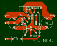
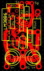
A few small changes:
- Found out how to create my own library elements, the lm3886 now has the correct pin layout & spacing.
- Moved GND pin to the middle, looks more like a star now.
- Moved mute resistor so it is completely below the LM avoiding shortcircuit with the heatsink.
- Added parts for Zobel network.
- Boardsize is 5 * 4 cm, 1 euro card can accomodate 8 of these pcbs.
Image now is smaller too, just 25k
Attachments
i think you better put also the holes not in use for the PCB in the LM3886 legs,
like every IC design, you put the full package detail...because if u dont drill that you just need to cut legs...
11 holes i assume?
if u have the schematic i am looking for a good & max.usage of this chip for max. power
thanks
like every IC design, you put the full package detail...because if u dont drill that you just need to cut legs...
11 holes i assume?
if u have the schematic i am looking for a good & max.usage of this chip for max. power
thanks
Morbid said:i think you better put also the holes not in use for the PCB in the LM3886 legs,
like every IC design, you put the full package detail...because if u dont drill that you just need to cut legs...
11 holes i assume?
if u have the schematic i am looking for a good & max.usage of this chip for max. power
thanks
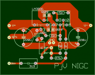
There were 11 pins to start with

I am going to cut pins 2, 6 & 11, mainly because I need the extra space for wider traces.
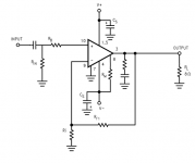
I'm basically using the schema as in the datasheet.
Some parts values have changed, and since I don't like elco's in the signal path I have moved the DC blocking cap to the input.
Partlist for this pcb:
Rin: 47k
Rb: 1k
Ri: 1k2
Rf1: 18k
Rm: 22k
unnamed 1E for zobel network
Cs(2x): 220uF elco + 100nF SMD
unnamed 3u3 cap @ input
unnamed 100nF for zobel network
Attachments
ok, well still i dont recommand cutting legs....
even if they are NC in the inside schematic there can be errors.
like if someone takes this PCB layout and cut the wrong leg
or the chip itself can be less stable (phisicaly)....
u can still bridge legs 1 and 5 without hurting leg 3...
b.t.w how u make the PCB after you draw it?
even if they are NC in the inside schematic there can be errors.
like if someone takes this PCB layout and cut the wrong leg
or the chip itself can be less stable (phisicaly)....
u can still bridge legs 1 and 5 without hurting leg 3...
b.t.w how u make the PCB after you draw it?
Squadra,
I agree with morbid, cutting of the pins is not a good idea. But if you want to do it, at least try to get the right pinnumbering on the chip, now it is quite confusing and you can bet somebody, sometime, maybe even you, will measure the wrong things or make a wiring mistake.
Question: I assume that one of the holes in the star ground is for the speaker return? Do you have a ps with a center tap? If you have two separate supplies, it would be good to run the returns of both to the star ground, then you need one more hole.
BTW Nice layout, looks pretty optimal to me.
Jan Didden
Morbid,Morbid said:u can still bridge legs 1 and 5 without hurting leg 3...
b.t.w how u make the PCB after you draw it?
If I don't cut pin 2 and leave 3 inline then the trace between pin 1 and 5 will be very small, too small for me.
I have returned pin 11, there was no reason to cut that one.
I will send the gerberfiles to a company that creates pcbs, I have no means of creating the pcbs myself.
janneman said:Squadra,
I agree with morbid, cutting of the pins is not a good idea. But if you want to do it, at least try to get the right pinnumbering on the chip, now it is quite confusing and you can bet somebody, sometime, maybe even you, will measure the wrong things or make a wiring mistake.
Question: I assume that one of the holes in the star ground is for the speaker return? Do you have a ps with a center tap? If you have two separate supplies, it would be good to run the returns of both to the star ground, then you need one more hole.
BTW Nice layout, looks pretty optimal to me.
Jan Didden
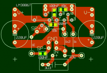
Thanks Jan,
Speaker return?
I plan on using a PS with separate grounds for V+ & V-.
Together with the speaker return I need 4 connections at the star ground.
So, again a new version
Attachments
Upupa Epops said:Lead not input ground throuth output ground, but beside by independent line to the middle of PS. Get input cap to the middle of PCB commonly with input groung. After that all will be OK
I have interpreted 'the middle of PS' as the center of the star ground. Is that correct?
Your tips lead to the newest attachment
Tnx,
Pj
Attachments
Getting better all the time. You may want to put the input gnd pad close to the input hot pad, makes it easier to solder the screened cable from the input. Run this pad with a short track to the start gnd.
The speaker output pad seems floating, or is there a jumper? Anyway, move the speaker pad to the right side of the electrolytic. Avoids speaker current under the cap. Also, move the V+ and V- pads closer to the chip, above the elcap, makes your pcb more compact and avoids unnessesary track length.
Jan Didden
janneman said:Getting better all the time. You may want to put the input gnd pad close to the input hot pad, makes it easier to solder the screened cable from the input. Run this pad with a short track to the start gnd.
The speaker output pad seems floating, or is there a jumper? Anyway, move the speaker pad to the right side of the electrolytic. Avoids speaker current under the cap. Also, move the V+ and V- pads closer to the chip, above the elcap, makes your pcb more compact and avoids unnessesary track length.
Jan Didden
Upupa & Jan, thanks for the comments & compliments, keep them both coming
Pin 3 of the LM3886 is bent a little forward and is soldered in the hole marked '3' in the speaker trace.
I will redo the design, guess I can go to 5 x 3 cm for the complete pcb.
Maybe it would be a good idea to move the lm3886 to the side of the pcb, although that would require the use of a wire for V-?
Pj
You can do it without jumpering the power tracks.
This is 25x45mm or thereabouts. (grid is 1/10 inch or 2.54mm)
It has been recommended that R3 go to power ground vs. Signal ground and I'm tweaking to this end. Also was suggested to eliminate Cb on this layout. The only reason I post here is to show it *can* be done. My own experience (or, I should say relative lack of experience) has me a little uncomfortable with anyone actually using my designs. (I've been working on this for a week or two and never had done PCBs before - but many have helped here, including Pedja - quite a helpful bunch, to which I am grateful). To that end, and to minimize the PCB size some, I have moved the zobel off-board (a pad for one end of the cap, one end of the R - a little P2P seems acceptable for a circuit most don't even use) and put the output resistor sideways (keeps the output away from the input). This is also intended for use with a regulated power supply, hence less room for power caps. I've also rotated the power caps 90 degrees (clockwise for V-, counter-clockwise for V+) to move the pins closer to the chip. Without the zobel or Cb in the network, this is closer than this version would allow.
Note, there *is* a jumper here, but it is used to connect Signal with Power ground, a connection that is almost always suggested to be "difficult" if that's an acceptable term. So, in this case, the disadvantages of a jumper end up being an advantage.
keep at it.
One thing that has come up that I'm curious about - is there a problem with running a trace through one of the unused pins on the chip without removing the pin? It seems to me it wouldn't be a good idea, but asking never hurt anyone... I hope.
C
This is 25x45mm or thereabouts. (grid is 1/10 inch or 2.54mm)
It has been recommended that R3 go to power ground vs. Signal ground and I'm tweaking to this end.
Also was suggested to eliminate Cb on this layout. The only reason I post here is to show it *can* be done. My own experience (or, I should say relative lack of experience) has me a little uncomfortable with anyone actually using my designs. (I've been working on this for a week or two and never had done PCBs before - but many have helped here, including Pedja - quite a helpful bunch, to which I am grateful). To that end, and to minimize the PCB size some, I have moved the zobel off-board (a pad for one end of the cap, one end of the R - a little P2P seems acceptable for a circuit most don't even use) and put the output resistor sideways (keeps the output away from the input). This is also intended for use with a regulated power supply, hence less room for power caps. I've also rotated the power caps 90 degrees (clockwise for V-, counter-clockwise for V+) to move the pins closer to the chip. Without the zobel or Cb in the network, this is closer than this version would allow.Note, there *is* a jumper here, but it is used to connect Signal with Power ground, a connection that is almost always suggested to be "difficult" if that's an acceptable term.
So, in this case, the disadvantages of a jumper end up being an advantage.keep at it.
One thing that has come up that I'm curious about - is there a problem with running a trace through one of the unused pins on the chip without removing the pin? It seems to me it wouldn't be a good idea, but asking never hurt anyone... I hope.
C
Upupa Epops said:To squadra : Now is it more better
Hi Upupa,
The newest version is attached, it is more symmetrical.
cjd said:You can do it without jumpering the power tracks.
This is 25x45mm or thereabouts. (grid is 1/10 inch or 2.54mm)
It has been recommended that R3 go to power ground vs. Signal ground and I'm tweaking to this end.
Note, there *is* a jumper here, but it is used to connect Signal with Power ground, a connection that is almost always suggested to be "difficult" if that's an acceptable term.
keep at it.
One thing that has come up that I'm curious about - is there a problem with running a trace through one of the unused pins on the chip without removing the pin? It seems to me it wouldn't be a good idea, but asking never hurt anyone... I hope.
C
Hi cjd,
With your 2 weeks you are far more experienced than I am, this is my 3rd day as pcb designer
There are indeed a lot of people helping eachother here, I've learned a lot just lurking.
If I'm correct then R3 is part of the feedback network, it doesn't seem right to 'polute' that with garbage from the power.
Of course I could be mistaken, I'm no expert, that's for sure
The attached PCB is 50 * 35 mm, I've read that at least 2 mm should be left for cutting the pcbs.
That's 46 * 31 mm effective board area.
I made a comprimise, there is now a trace below the LM3886 for V- and it can be jumpered.
If there is any danger in connecting a NC pin to some other trace I don't know.
I decided to avoid any problems and read Reserved instead of NC, so I will cut pin 2 & 6.
Thanks for your input,
Pj
Attachments
There is no danger to connect the NC-pins, because they are not connected (I tried it with one of my first boards).
Maybe it is the better idea, than to cut some pins : they help to get some heat out of the chip. So, give them some copper and solder, just a little bit, and dont cut them!
Franz
Maybe it is the better idea, than to cut some pins
: they help to get some heat out of the chip. So, give them some copper and solder, just a little bit, and dont cut them!Franz
The universe is balanced, not symmetrical.
Moving V- to the same "side" of the board as V+ cuts out a lot of trace on the V- side with the 3886.
And, R3 *is* part of the feedback and, as it was explained to me, that should all go directly to the main (power) ground star (vs Signal ground, which is then attached to the power grund star).
It does look good though. It won't be something you can mount up to the side of the case or similar as is common, but that's not a problem by itself.
Franz G: I like hearing I can run traces through NC pins. Helps keep paths shorter, and if there really is no reason to clip them it helps other ways (as you mentioned).
C
Moving V- to the same "side" of the board as V+ cuts out a lot of trace on the V- side with the 3886.
And, R3 *is* part of the feedback and, as it was explained to me, that should all go directly to the main (power) ground star (vs Signal ground, which is then attached to the power grund star).
It does look good though. It won't be something you can mount up to the side of the case or similar as is common, but that's not a problem by itself.
Franz G: I like hearing I can run traces through NC pins.
Helps keep paths shorter, and if there really is no reason to clip them it helps other ways (as you mentioned).C
And now for something completely different
The pcb for the PS buffering...
I am going to use 3 * 1000uF/63 for each rail.
That should be enough for a single LM I guess.
The rectifiers will be connected to a metal plate for cooling, so no pcb is needed for that.
Thanks again everybody for your input.
So far it has been a lot of fun
The pcb for the PS buffering...
I am going to use 3 * 1000uF/63 for each rail.
That should be enough for a single LM I guess.
The rectifiers will be connected to a metal plate for cooling, so no pcb is needed for that.
Thanks again everybody for your input.
So far it has been a lot of fun
Attachments
For this output power use standard bridge such as KBUJ 8, which you can give directly to this PCB. Don't belive to anything who will say to you, that you need some exotic ones - it says only ones, who don't know design correct PCB. With bridge on PCB commonly with elyts you get shortly wires, which is more significant than any exotic bridge or diodes.
- Status
- This old topic is closed. If you want to reopen this topic, contact a moderator using the "Report Post" button.
- Home
- Amplifiers
- Chip Amps
- pcb layout for lm3886