More and more good pcb design has maked.let's make a pcb based gc becomes simple,beautiful and steady.
If us minimize a chip amp,as possible as compact,integrate the PCB,chips,components and heat sink in a block module.all interfaced directly to the pcb.no wire,no distance...
this is a mad ideas,I think it can over and over the original GAINCARD's layout projects.
first plan please see this link:http://diyaudio.com/forums/showthread.php?postid=382229#post382229
peter,and all gc gays,please")
If us minimize a chip amp,as possible as compact,integrate the PCB,chips,components and heat sink in a block module.all interfaced directly to the pcb.no wire,no distance...
this is a mad ideas,I think it can over and over the original GAINCARD's layout projects.
first plan please see this link:http://diyaudio.com/forums/showthread.php?postid=382229#post382229
peter,and all gc gays,please
digi01 said:
peter,and all gc gays,please
I take it you mean guys, not gays here, right?
(I can't even manage to spell 'not' right today)
One thing which I have thogut about trying to do with the LM4780 design was to see how much better you could make the PCB using a four layer board. This way, you could have on plane each dedicated to V+, V- and ground, with a whole layer left over for the signal routting. The only thing I have to say against this is that it may cost quite a lot more to get the four layer boards produced (although, I'm sure it could still be done for less than $10, per board for each chip, and the PSU could still be just single sided). Also, this would mean that I realy would have to spend some time learning how to use protel, as the free version of eagle I normaly use will only do two signal layers.
The second thing that I have thought about has kind of already been brought up in the other thread for the LM4780 boards, which is to try and use SMD (some of the large types anyway) components for the non-audio signals on the PCB, such as any possibly mutting circutry that needs to be included. As, this should in theory reduce the cos of those components if it is for a group order, and allow a smaller PCB design as well.
The second thing that I have thought about has kind of already been brought up in the other thread for the LM4780 boards, which is to try and use SMD (some of the large types anyway) components for the non-audio signals on the PCB, such as any possibly mutting circutry that needs to be included. As, this should in theory reduce the cos of those components if it is for a group order, and allow a smaller PCB design as well.
One thing which I have thogut about trying to do with the LM4780 design was to see how much better you could make the PCB using a four layer board.
actuality,we can stack the boards.It is not necessary to use a expensive four layer board design.
I had the other styles designs of a serise 4780 layout projects, I do not want to repeat this direction...
Critique
Digi,
Please consider the following, but realize I didn't have much time to spend looking at it.
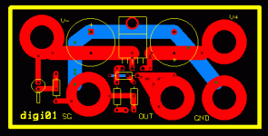
What is the advantage of providing big plugs that connect to another "pcb" to distribute V+, V-, gnd and so on? I guess your concept is to plug one board into another, right? I guess this would be great for testing lots of pcb's coming off the assembly line. You could just plug them in, test them and send them on.
But I can't see the advantage for our needs. In fact, the placement of the plugs has caused all of the supply and ground lines to be way too long and you're sharing too many connections along the trace leading to ground.
I can see the benefit of consolidating everything on one pcb for 2 or 4 channels and it makes sense to me to try and put an rca jack and 2 speaker jacks directly on the pcb, but then you would have serious limits on how to place the unit in a back panel of your box. But I think a small self-contained module like that might be fun anyway.
-Robert
Digi,
Please consider the following, but realize I didn't have much time to spend looking at it.
What is the advantage of providing big plugs that connect to another "pcb" to distribute V+, V-, gnd and so on? I guess your concept is to plug one board into another, right? I guess this would be great for testing lots of pcb's coming off the assembly line. You could just plug them in, test them and send them on.
But I can't see the advantage for our needs. In fact, the placement of the plugs has caused all of the supply and ground lines to be way too long and you're sharing too many connections along the trace leading to ground.
I can see the benefit of consolidating everything on one pcb for 2 or 4 channels and it makes sense to me to try and put an rca jack and 2 speaker jacks directly on the pcb, but then you would have serious limits on how to place the unit in a back panel of your box. But I think a small self-contained module like that might be fun anyway.
-Robert
- Status
- This old topic is closed. If you want to reopen this topic, contact a moderator using the "Report Post" button.
- Home
- Amplifiers
- Chip Amps
- Trying to improve on a PCB based chip amp performances