I'm busy designing a pair of DRV134 input boards to convert each stereo channel into balanced outputs for four LM3886 boards to drive (see overall design here).
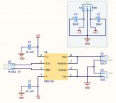
The simple schematic for the DRV134 board is attached. The board will be driven by an external power supply, supplying ±15V for the DRV134s and ±28V for the LM3886es.
Question:
Should all the GNDs here be connected? Or rather, is there any reason not to connect the power supply GND (coming into the board via X4) and the signal GNDs (the input and outputs, X2 and X3)? Would a big, chunky ground plane be fine to use to connect all the grounds here?
Attachments
Should all the GNDs here be connected?
The grounds must all be connected together, including pin #3.
Do a search for "digi01" (I think) as he did some pcb's for that a while back and posted the files ( again I think).
Quoting myself...

BALANCED LINE DRIVER,PCB layout share
The grounds must all be connected together, including pin #3.
Cool, thanks!
There's no PCB to criticize...
Tom
PCB incoming
Awesome, thanks for the reference. Bang on, pretty much! I'll post my PCB shortly - I don't think I'm far off this one already. Nice!
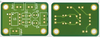
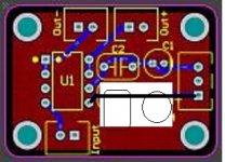
Right, PCB attached. I realise this is an extremely simple circuit and PCB, but I'm still learning and would value feedback as I go
Any feedback would be welcome!
...
- I've kept all the traces thick (36mil), because there's plenty of room to do so.
- I've used 0.1uF WIMA poly "red box" caps for bypassing, as this is what I have at hand.
- Likewise for the 10uF electrolytics
Any feedback would be welcome!
...
Attachments
Nice work.
If you don't mind upsetting the symmetry of the component placement, consider moving C3 and C2 down a bit to get them closer to the power pins on U1. That may or may not make a difference in this case, but it's good practice.
The power traces are very (in my opinion, unnecessarily) close to other pads. It appears there is room to move them away and, at the same time, if there's room, make them even thicker.
This is a small thing and is not a big issue for hobbyists, but in a hand placed production environment it matters. Place the electrolytic capacitors so their polarity is in the same direction.
That's all the nit picking I can come up with.
If you're going to make a differential line driver, you might as well make the output ... differential. That means the output traces are equal in length and tightly coupled. Also, the DRV134 features sense inputs to sense the voltage on the output of the chip. Why not use them to compensate for the drop across the trace to the output connectors?
I suggest using pours rather than traces for the supply connections.
You've connected the dots, but it takes more than connecting the dots to form a good layout.
I also suggest cleaning up the silk screen so you don't have legend (+ on the 10uF caps, for example) overlapping with the outlines of components.
I generally prefer to have polarized components arranged in the same orientation across the board. So + on your caps would point in the same direction if I was to make it. It really makes assembly easier and makes correct assembly easier to verify. One could argue that this is nit picking for DIY, but you said you wanted to learn...
Note the layout guidelines on Page 17 of the DRV134 Data Sheet. You may find that you're missing a component in your circuit.
Tom
Last edited:
Thanks @farley!
Ah, the old "symmetry vs. good layout" chestnut 2 very good pieces of feedback, will do so.
(snip)
The power traces are very (in my opinion, unnecessarily) close to other pads. It appears there is room to move them away and, at the same time, if there's room, make them even thicker.
This is a small thing and is not a big issue for hobbyists, but in a hand placed production environment it matters. Place the electrolytic capacitors so their polarity is in the same direction.
(/snip)
Ah, the old "symmetry vs. good layout" chestnut
2 very good pieces of feedback, will do so.Ah, the old "symmetry vs. good layout" chestnut
Your current layout isn't symmetric anywhere. Especially not where it matters (the IC output).
Tom
Thanks@tomchr! Nah, there's no such thing as too nitpicky when you're still learning. Can't break the conventions until I know them!
Interesting. Out of curiosity, how much of a difference does ever-so-slightly longer or shorter traces here make? Additionally, I can see the value in keeping the output traces identical in length, but can I ask what you mean by "tightly coupled" in this context?
Even more interesting. How would this be achieved? I don't see much in the way of examples in the reference schematics where this is implemented - could you briefly explain the implementation and how this works? (I'm imagining some capacitance between the sense and output pins, but could be barking up the wrong tree.)
Cool, will do! Would you say that in general it's more beneficial to have both GND and power planes, even for distances this small?
Thanks very much!
...That means the output traces are equal in length and tightly coupled.
Interesting. Out of curiosity, how much of a difference does ever-so-slightly longer or shorter traces here make? Additionally, I can see the value in keeping the output traces identical in length, but can I ask what you mean by "tightly coupled" in this context?
...the DRV134 features sense inputs to sense the voltage on the output of the chip. Why not use them to compensate for the drop across the trace to the output connectors?
Even more interesting. How would this be achieved? I don't see much in the way of examples in the reference schematics where this is implemented - could you briefly explain the implementation and how this works? (I'm imagining some capacitance between the sense and output pins, but could be barking up the wrong tree.)
I suggest using pours rather than traces for the supply connections.
Cool, will do! Would you say that in general it's more beneficial to have both GND and power planes, even for distances this small?
Thanks very much!
Interesting. Out of curiosity, how much of a difference does ever-so-slightly longer or shorter traces here make? Additionally, I can see the value in keeping the output traces identical in length, but can I ask what you mean by "tightly coupled" in this context?
Tightly coupled means that the two traces run close together so they see the same electromagnetic field from the external world.
For audio, the difference in length doesn't matter much, but you want the traces to run as a differential pair rather than as two traces.
Even more interesting. How would this be achieved?
I suggest looking up Kelvin sensing. Another search term would be remote sensing.
From Wikipedia: Four-terminal sensing - Wikipedia
Remote sensing is used in power supplies, but applies equally here. Here's an article from EDN on the topic: https://www.edn.com/electronics-blo...wer-supply--Remote-Sense--mistakes---remedies
Tom
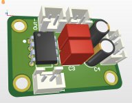
abza, what software do you use to render the PCB images?
@BabyDontHertzMe - I use CircuitStudio for PCB design which has a built-in 3D renderer, but also use the ZofzPCB - a freeware 3D Gerber viewer
@BabyDontHertzMe - I use CircuitStudio for PCB design which has a built-in 3D renderer, but also use the ZofzPCB - a freeware 3D Gerber viewer
Thank you for the info
. I use ZofzPCB occasionally, but will give the CircuitStudio trial a go.Something like that
Exactly. Do the same for C1 and C2 and it should look a lot cleaner
- Status
- This old topic is closed. If you want to reopen this topic, contact a moderator using the "Report Post" button.
- Home
- Amplifiers
- Chip Amps
- Critique my PCB! DRV134 board