LM1875, TDA2030/40/50 share same pinout aqnd PCBs are mutually compatible.
There´s dozens of PCB designs for them floating out there, if not hundreds, certainly a few even here, Google is your friend.
Do your homework, the *first* page if found showed ***96*** images of suitable PCBs.
There´s dozens of PCB designs for them floating out there, if not hundreds, certainly a few even here, Google is your friend.
Do your homework, the *first* page if found showed ***96*** images of suitable PCBs.
Split rail is better than a single supply voltage if you do not use BTL coupling. The reason is, you else need a good electrolytic capacitor in series with the speaker when using ground as one terminal for the speaker (for single supply voltage).
With BTL configuration you do not use ground for your speaker.
With BTL configuration you do not use ground for your speaker.
True... But it is my impression that TDA's are a bit more layout-sensitive. Eager to oscillate if something isn't quite PC....
LM1875, TDA2030/40/50 share same pinout aqnd PCBs are mutually compatible.
...
Dear Vrystaat, I am somewhat worried that you picked 3 different PCB designs, incompatible with each other, and you seem to treat them as if they were the same.
And none of them offers a "Bottom only / tracks only / ready to iron artwork" to make the actual PCB by the iron on Toner Transfer method which is the most practical for home hobbyists.
Commenting on these:
1) Designs 1 and 2 look reasonable and I don´t find errors , first board is fine but they complicated the design somewhat, parts are over rated, probably trying to "improve" it, but problem is that IF you get the ready to transfer drawing spacing between tracks is on the narrow side for iron method, which "smears" toner a little.
I like the second design very much, improvements here are real (antiparallel caps in NFB and output inductor) and if you find the transferrable drawing, that would be my choice.
Tracks are again widely separated so a little smearing is not a problem.
The third design looks amateurish and clumsy, plus it´s incomplete, not my choice.
2) so in a nutshell I suggest you google what I did:
tda2030 lm1875 pcb - Google Search
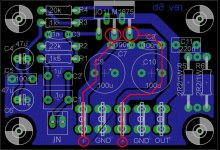
Look for something *similar* to this:

or this:

although in this case, after ironing I would double the thickness of the thinner tracks with solvent based marker, there is ample space and it´s safer/better.
You need to have a fine point "Sharpie" type marker anyway, because one problem with transfer ironing is that sometimes small cracks appear, or very thin tracks disappear, both corrected with the solvent type ink they carry.
3) best would be finding a page which shows a full project with step by step instructions (you might also find a relevant YT Video) , this is a very popular project")
Or at least a page which shows: actual schematic, parts layout and black-on-white PCB image for toner transfer.
Plan B: buy a ready made PCB on EBay but make certain they send you the actual schematic (there are small variations) , and the layout.
And none of them offers a "Bottom only / tracks only / ready to iron artwork" to make the actual PCB by the iron on Toner Transfer method which is the most practical for home hobbyists.
Commenting on these:
1) Designs 1 and 2 look reasonable and I don´t find errors , first board is fine but they complicated the design somewhat, parts are over rated, probably trying to "improve" it, but problem is that IF you get the ready to transfer drawing spacing between tracks is on the narrow side for iron method, which "smears" toner a little.
I like the second design very much, improvements here are real (antiparallel caps in NFB and output inductor) and if you find the transferrable drawing, that would be my choice.
Tracks are again widely separated so a little smearing is not a problem.
The third design looks amateurish and clumsy, plus it´s incomplete, not my choice.
2) so in a nutshell I suggest you google what I did:
tda2030 lm1875 pcb - Google Search
Look for something *similar* to this:
or this:
although in this case, after ironing I would double the thickness of the thinner tracks with solvent based marker, there is ample space and it´s safer/better.
You need to have a fine point "Sharpie" type marker anyway, because one problem with transfer ironing is that sometimes small cracks appear, or very thin tracks disappear, both corrected with the solvent type ink they carry.
3) best would be finding a page which shows a full project with step by step instructions (you might also find a relevant YT Video) , this is a very popular project
Or at least a page which shows: actual schematic, parts layout and black-on-white PCB image for toner transfer.
Plan B: buy a ready made PCB on EBay but make certain they send you the actual schematic (there are small variations) , and the layout.
Last edited:
- Status
- This old topic is closed. If you want to reopen this topic, contact a moderator using the "Report Post" button.
- Home
- Amplifiers
- Chip Amps
- LM 1875 layout