TINA-Ti Simulation error?
Hey guys, back at it again with this amplifier this time just trying to put everything into the simulation.
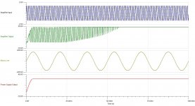
The problem I am having is that amplifier doesn't see the output of the full bridge amplifier properly. As shown in the graph the power supply is outputting a smooth ~30VDC, however the amplifier isnt seeing this.
Any help would be appreciate as I think its the simulation software.
Hey guys, back at it again with this amplifier this time just trying to put everything into the simulation.
The problem I am having is that amplifier doesn't see the output of the full bridge amplifier properly. As shown in the graph the power supply is outputting a smooth ~30VDC, however the amplifier isnt seeing this.
Any help would be appreciate as I think its the simulation software.
Attachments
Last edited:
Hey guys, I was wondering whats up with this? I find no reason why it shouldnt be working.
The simulation seems fine however its not at the same time? Maybe I am over looking something any help would be amazing thanks.
You are overlooking the setup times of your slow biasing networks.
It might take several seconds until the amp is in a stable condition.
I don't think that's a simulation error. I bet the DC bias on the non-inverting input of the LM1875 is drifting to the point where the amp starts clipping.
Given that your supply voltage starts at zero, it will take some time for the DC bias on C2 to stabilize, so you either need to let the simulation run that long or set up the simulation differently.
You mention that the amplifier output is stable after 1 second, so one approach could be to simulate for 1.1 seconds and only save the last 0.1 seconds of the results. You can set that up in the transient simulation dialog. That'll make it faster to view the graph and might improve the simulation speed also.
My choice would be to scrap the transformer, rectifier, and supply cap and use a DC voltage source for the supply. This will allow the simulator to work out the steady-state DC bias on the various capacitors. You'll likely see much better behaviour then.
What you're seeing could be real, though. It is entirely possible that your amplifier will start up like that in reality. That would warrant some prototyping as it doesn't look gentle to any speaker attached to the amp.
I don't have any experience with the LM1875 simulation model, but am intimately familiar with the LM3886 model in TINA-TI. The LM3886 neglects anything related to the supply pins - including the supply current!! If the LM1875 model is similar, it is of limited use to determine anything supply-related, aside from maybe the clipping behaviour.
My advice: Get it working with a DC source in the simulator and prototype the rest in the lab. Be mindful of the startup, as that behaviour could be real.
Tom
Try placing the 2200uF capacitor after the output (C6 in the TI datasheet).
Good catch. You'll definitely need the DC blocking cap if you're going to use a single supply.
Just as well this is a simulation. Your 8ohm speaker would have released its magic smoke with 30VDC at the output.
Not necessarily. It could be a 1 kW capable sub for all we know.
")
The LM model might be reacting to the high current and shutting down.
I highly doubt that's modelled. Besides, the current limiter in the LM1875 doesn't shut down the chip. I just limits the peak current. Also, if the chip was actually in shutdown, it wouldn't produce 30 V on it output. It'd produce 0 V.
Tom
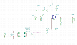
Sorry for bothering you guys again, however whats the purpose of C7 here. The only think I can think of is that in DC analysis it stops the DC from going into ground however why is that a good thing? Allowing DC not being sinked into ground. Is it due to creating a voltage drop across R6 and R7 thus having to do something with the Current Offset?
This also creates a filter, how does a filter improve the situation and
I have heard things that this reduces the gain at lower frequencies, but isn't lowering the input voltage the same thing?
This also creates a filter, how does a filter improve the situation and
I have heard things that this reduces the gain at lower frequencies, but isn't lowering the input voltage the same thing?
An externally hosted image should be here but it was not working when we last tested it.
whats the purpose of C7 here. The only think I can think of is that in DC analysis
it stops the DC from going into ground
A large capacitor between the feedback resistor and ground forces the amplifier's gain at DC to be unity (0dB).
It's part of the nfb loop. This can be useful for various reasons, like protecting the speakers, reducing
wasted power and speaker distortion at subsonic frequencies, automatically minimizing DC offset, etc.
Last edited:
You're absolutely right, can you maybe further explain how this happens,
and if I remove the said capacitor it drives my output voltage to 8pV
or somewhere really small.
The signal gain is the same formula as a noninverting op amp, (1+ R1/R2),
where R1 is the output to input resistor, and R2 is the resistor to ground.
However, with the capacitor in the circuit, the gain becomes
1+ R1/(R2 + 1/sC), where 1/sC is the capacitor's impedance.
When the 1/sC is small compared to R2 (at high frequencies),
the usual formula for gain, 1+R1/R2 results.
When the capacitor's impedance is large compared to R1
(at very low frequencies), the gain is 1+R1/(1/sC), or 1+ sCR1.
If the frequency is very small (near 0Hz), then s~0, and the
gain becomes 1 (0dB).
A DC input offset, from mismatched transistors, etc. is effectively a DC input signal,
so the unity gain at DC prevents it from being amplified excessively by 1+R1/R2.
Last edited:
how does the Zobel network/Thevin network affect the NFB
Capacitive loads can cause phase lag and reduce the amplifier's stability margin.
An output Zobel RC snubber circuit improves the amplifier's stability with capacitive loads.
The resistor of the RC reduces the amplifier's open loop gain in the critical area
of the high frequencies, while the capacitor of the RC preserves the amplifier's
open loop gain at lower frequencies.
Last edited:
Sorry, I meant I knew that I just want to use nodal analysis and see it through poles and zeroes how it affects the Gain phase.
Another question as well, sorry for bombarding you. Does this make sense to you?
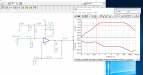
Shouldn't the Fc = 0.000159Hz? and not 1.05Hz? How do you alter the op amps Low and High frequencies
Another question as well, sorry for bombarding you. Does this make sense to you?
An externally hosted image should be here but it was not working when we last tested it.
Shouldn't the Fc = 0.000159Hz? and not 1.05Hz? How do you alter the op amps Low and High frequencies
Last edited:
Shouldn't the Fc = 0.000159Hz? and not 1.05Hz? How do you alter the op amps Low and High frequencies
The -3dB from the midband gain level would be at approx.
f = 1 / (2 x Pi x 10000 ohm x 0.000010 Farad) = 1.59Hz
The presence of the 10uF capacitor gives a 0dB gain shelf at DC and very low frequencies.
The gain then starts to rise from unity at approx. where 100k ohms = 1/sC, around 0.159Hz.
The gain then rises at about 20dB per decade up to 1.59Hz, and then the gain levels off
to a constant gain of (1+100k/10k).
The response looks like fig. 5 here. ActivLab
Last edited:
how do you know which filter applies their things first?
Oh I guess, since you're adding poles and its super imposed onto it.
is it just multiple filters just added together essentially?
The entire circuit has a transfer function, and a net response from it.
You can simplify calculation with approximations, in frequency regions
where a particular time constant dominates. The exact response requires
the entire circuit matrix calculation, though.
The C has a high impedance at low frequencies, and a low impedance at high frequencies.
If the circuit's poles and zeros are widely enough separated, you can use approximations
in the various frequency regions to get an idea of the overall response.
Control Systems/Bode Plots - Wikibooks, open books for an open world
Last edited:
Yeah, thats what I mean. You can pretty much super impose poles and zeros onto a bode plot.
do you take account all the High pass and low pass filters in the circuit then just do it?
Yes, though constructing a Bode plot by inspection takes some practice.
Bode Plot - online generator, examples, drawing rules, transfer function (magnitude and phase)
Last edited:
- Status
- This old topic is closed. If you want to reopen this topic, contact a moderator using the "Report Post" button.
- Home
- Amplifiers
- Chip Amps
- Purpose of a feedback Capacitor (Ci)