I know the world doesn't really need any more LM3886 designs but I'm getting some four layer boards made up for a pre-amp and as an experiment I thought I'd get a few chip amp boards made at the same time.
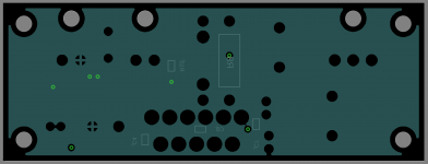
Top layer is all signal, 2nd layer is a signal ground pour, 3rd is power ground and the bottom is DC. As layers 2 & 3 are just pours I've only posted pics of the top and bottom.
Any comments welcome.
One question... what do you guys use to measure THD & Noise? I have an HP334A distortion analyser (which has had a hard life) and an Analog Discovery II, but both of those seem to top out at about 75-80dB THD measurements. I'm not willing to spend thousands on an analyser yet but I've had my eye on the QA401 by Quantasylum.
Attachments
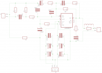
It would be interesting to have layers 2 and 3. How the ground is laid out and where signal and power ground meet are quite important.
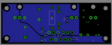
About and parts and via: it's good practice to use multiple via and thick tracks from pad to via, to minimize inductance. Particularly so for bypass caps.
For measurements on a budget, have you considered Pete Millet interface with a good sound card?
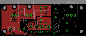
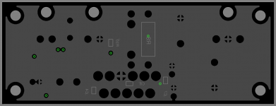
BTW, am I the only one to find it harder to evaluate PCB when the bottom pic is mirrored?
About and parts and via: it's good practice to use multiple via and thick tracks from pad to via, to minimize inductance. Particularly so for bypass caps.
For measurements on a budget, have you considered Pete Millet interface with a good sound card?
BTW, am I the only one to find it harder to evaluate PCB when the bottom pic is mirrored?
Thanks for the suggestions on test equipment... I'll do a bit of reading. As for the other pics, please see attached (with an un-mirrored bottom layer ") ). Grounds join at the via by R10... I couldn't decide whether this should be close to the speaker return or the decoupling caps.
). Grounds join at the via by R10... I couldn't decide whether this should be close to the speaker return or the decoupling caps.
). Grounds join at the via by R10... I couldn't decide whether this should be close to the speaker return or the decoupling caps.Attachments
Honnest to God question, not a trap: what's the point of the signal ground pour going all over the pcb ? There are no loops running above or through it for most of the board. Don't you risk capacitive coupling of noise between the overlapping power and signal gnd ? Wouldn't that copper better used by shifting the right half of the signal gnd pour layer to the power lines ?
I'm asking because that's a question that popped up in another layout thread and wasn't really answered.
I'm asking because that's a question that popped up in another layout thread and wasn't really answered.
If I remember right it has been mentioned multiple times on this forum that it would be wise to use bigger physical size resistor for feedback resistor R3 due to thermal effects. This resistor can dissipate around 50mW (my estimate) at peak output voltage swing and in small 0805 size with typical 25ppm tempco it can by itself add measurable THD due to thermal modulation of its resistance.
Regards,
Oleg
Regards,
Oleg
Thanks for the responses,
00940 - I didn't think capacitive coupling of noise would be a problem - it's not been in the past... willing to be educated though. Just figured I'd go for big pours with minimum impedance to ground (I get your point that the signal only covers 1/3 of the top layer though).
OlegSh - I can get a 250mW 0.1% thin film in that package.
One question... what do you guys use to measure THD & Noise?
APx525
QA401 by Quantasylum.
That'd be on my list if I didn't already own the 525.
I couldn't decide whether this should be close to the speaker return or the decoupling caps.
See here: LM3886 chip amp grounding.
Just figured I'd go for big pours with minimum impedance to ground (I get your point that the signal only covers 1/3 of the top layer though).
That's usually a good approach. Maximizing the VCC and VEE connections is usually worthwhile as well, though with a single LM3886, you don't gain that much by running those in planes.
OlegSh - I can get a 250mW 0.1% thin film in that package.
Beware of the voltage coefficient of the feedback resistor as well. This is especially true for the SMD resistors.
Tom
This resistor can dissipate around 50mW (my estimate) at peak output voltage swing and in small 0805 size with typical 25ppm tempco it can by itself add measurable THD due to thermal modulation of its resistance.
Beware of the voltage coefficient of the feedback resistor as well. This is especially true for the SMD resistors.
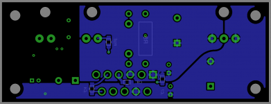
I'd like to stick to the 0805 package if I can - I'm thinking of the following options:
1) 1/4W 5ppm Vishay - best temp coefficient and power rating I can find in this package (a bit pricey at £5 a pop but I'm willing to give them a go)
2) 1W 25ppm Vishay - to make the most of these I'll need to increase the pad sizes and possibly add some thermal relief to the board. (a bit cheaper)
3) Stack two or more standard 0.1 % thin film resistors - I don't know how efficiently stacked resistors dissipate heat.
I guess I could keep the layout the same and try all three approaches. I'm thinking I'll need to make that investment in test gear to measure the results though.
I'd like to stick to the 0805 package if I can - I'm thinking of the following options:
Why the allergy to 1210 esque sizes? It buys you a lot more dissipation and you're not hurting for selection.
I guess I could go with a size up... this 1206 might fit the bill at 14W and 10PPMWhy the allergy to 1210 esque sizes? It buys you a lot more dissipation and you're not hurting for selection.
Blimey... that'd have had more of an impact than my choice of resistors.The polarity of C6 and C11 are incorrect.
Thanks both.
Last edited:
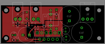
Watch the angle of entry into the pads. Some of the entries are at really acute angles. Your PCB manufacturing place will hate you. As will your PCB assembly place. For DIY it doesn't matter but for mass production, I'd clean it up. The curved traces do nothing for you other than look pretty.
Tom
Tom
Okay I didn't realise that... I assume you're talking about mute to R7 and R1 to C1(and possibly others). Why will they hate me?Watch the angle of entry into the pads. Some of the entries are at really acute angles. Your PCB manufacturing place will hate you. As will your PCB assembly place. For DIY it doesn't matter but for mass production, I'd clean it up.Tom
Yep... I knowThe curved traces do nothing for you other than look pretty.Tom
I think you're right... no reason not to.I'd really double up on that via to gnd for c7. Too bad to have good big planes and then have a highish inductance connection to it.
Thanks for the feedback both.
On acute angles, here's what pcbcart says:
2. Acid traps
When two traces are joined at a highly acute angle it is possible that the etching solution used to remove copper from the blank board will get "trapped" at these junctions. This trap is commonly referred to as an acid trap. Acid traps can cause traces to become disconnected from their assigned nets and leave these traces open circuited. The issue of Acid traps has been reduced in recent years by fabricators switching to the use of photo activated etching solutions. So, while it is still a good idea to make sure that your traces do not meet acute angles, the issue is less of a worry than it had been in the past.
Is the problem having to use a larger size, or having to change the layout?I'd like to stick to the 0805 package if I can - I'm thinking of the following options:
There's the idea of replacing it (just glancing, there's barely enough rooom) two 0805s each of half the resistance in series. That way they each get half the voltage and dissipate half the power.
For the assembly aspect: If one pin of a component has a big fat trace connecting to it and a skinny trace at the other end, the fat trace will remove far more heat than the skinny trace. This may cause the solder at one junction to flow well while the other end has a cold solder joint (or hasn't flowed at all). That's why we use thermal reliefs.
Not an issue with DIY and not much of an issue with passives. With tight pin pitch parts, such as LLPs and BGAs, the part may actually shift during reflow as it gets pulled by the surface tension of the molten solder, which causes all sorts of fun effects.
Tom
Not an issue with DIY and not much of an issue with passives. With tight pin pitch parts, such as LLPs and BGAs, the part may actually shift during reflow as it gets pulled by the surface tension of the molten solder, which causes all sorts of fun effects.
Tom
- Status
- This old topic is closed. If you want to reopen this topic, contact a moderator using the "Report Post" button.
- Home
- Amplifiers
- Chip Amps
- Four Layer LM3886 Layout