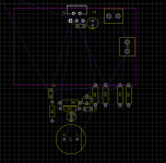
Hey guys, I just want a second opinion here as this is legit my first time doing this. I tried to keep everything close to the chip as possible. I tried to drive home the concept of the Star ground and hopefully its right but here it is.
PCB + Schematic
J3 -(negative) is suppose be my star ground if it was hard to tell.
PCB + Schematic
J3 -(negative) is suppose be my star ground if it was hard to tell.
Last edited:
Hi crisroxmysoc,
I would suggest to make significantly wider traces for power and output networks. Also placing input connector right next to the power entry connector is not a good idea. I would rather move output connector next to the power entry point and move input connector away from it. One question, is it your design requirement to use a single rail power supply? The "start ground" as you implemented it has too high impedance to be a good reference point.
One more thing, C7 is now right in the way of a screw driver when you try to mount LM1875 to the heatsink...
Regards,
Oleg
Hi! Thank you, yeah I just changed the width of the power and output network forgot about that.
Its a limitation for my power supply being a single 30V.
Hmmm C7 is not in a way of a screw as the heatstink will be outside of the PCB and behind the chip if that makes any sense.
High impedance? I am not sure where the high impedance is coming from as thats the lowest potential in my circuit. Or I just dont understand anything. Is that not how you do a star ground?
If you mount LM1875 standing upright at 90 degree to the PCB then C7 is in the way of a screwdriver.
The high impedance is not related to the star point itself but to the traces which suppose to carry its reference potential to other nodes. The longer those traces are the higher is their impedance and any current passing through this impedance will create an error potential degrading your reference. I would recommend to use ground planes instead. One for the power and output network and one for the input and feedback network. Then connect the two together at the output connector ground pin since this is the point which you want to control - the output. You can have a look at LM3886 chip amp grounding. for more information on the grounding. Tom (tomchr@diyaudio) explains it in great detail and provides a lot of other information on chip-amp design.
The high impedance is not related to the star point itself but to the traces which suppose to carry its reference potential to other nodes. The longer those traces are the higher is their impedance and any current passing through this impedance will create an error potential degrading your reference. I would recommend to use ground planes instead. One for the power and output network and one for the input and feedback network. Then connect the two together at the output connector ground pin since this is the point which you want to control - the output. You can have a look at LM3886 chip amp grounding. for more information on the grounding. Tom (tomchr@diyaudio) explains it in great detail and provides a lot of other information on chip-amp design.
Last edited:

Agreed, I am just confused on how to actually GND things onto a PCB.
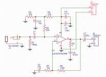
For example looking at this one. Isn't this star ground? TDA2003 Stereo Amplifier - EasyEDA.
Where I get confused at, if using a single power supply everything needs to meet at 0V, or the negative terminal of the power supply right? So do I isolate the lower current from the high current then route them individually to the 0V? and wouldn't the 0V be on the high current side already?
Well, not everything posted online is necessarily good, so be critical about what you see and read. There are examples of good designs on this forum. Just search for LM1875 in chip-amp forum and I am sure you'll find them.
For a general single polarity supply circuit the reference potential can be either of the polarities, but the common practice is a negative polarity.
Yes, you should isolate the high current path from the low current path and then connect them together at the common reference point which is 0V pin of the output connector. The rationale for doing so is that it lets you come close to the ideal relation between the input and the output potentials: Vout = Vin*gain where Vout is the output potential across the output connector pins and Vin is the potential across the input connector pins. In real life such ideal relation is impossible to achieve but you can come close to it. In reality, if your 0V reference is away from the output and on top of that your signal has high impedance path to that reference point too then the real equation you'll be looking at is Vout = (Vin + Vin_error)*gain + Vout_error, where Vin_error and Vout_error are the error potentials due to added impedances of input and output to the reference point. So the goal is to reduce Vin_error and Vout_error as much as possible by minimizing the impedance to the reference point for both the input and the output. Since input signal carries very little current its impedance to the reference point can be higher before it will become an issue while output with its high currents can generate significant error potential even across relatively low impedance. That is why it is better to use the 0V output pin as your reference point.
Is the overall ideal goal, is always keep traces as short as possible to the amp?
Have ground planes separating the high current from the low current?
and can someone verify if I am correct.
High current nodes - R3, C2/ R5 C5/ Speaker/ R7 C6?
Low Current nodes - Audio input/ R1
Is this correct?
Have ground planes separating the high current from the low current?
and can someone verify if I am correct.
High current nodes - R3, C2/ R5 C5/ Speaker/ R7 C6?
Low Current nodes - Audio input/ R1
Is this correct?
No. You need to upload pictures to diyaudio...
ahh now it will let me... here
Attachments
Is the overall ideal goal, is always keep traces as short as possible to the amp?
Traces by themselves are not the main problem, what really matters is the loop area which those traces create.
Have ground planes separating the high current from the low current?
No, just using the ground plane does not eliminate the problem.. You should follow the return currents and make sure that high current routes do not come close to the sensitive parts of the circuit.
High current nodes - R3, C2/ R5 C5/ Speaker/ R7 C6?
Low Current nodes - Audio input/ R1
R3, R4 and C2 set the mid supply potential for the non-inverting input and are part of the signal network. There is no high current through R3+R4 (22k+22k) network.
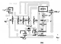
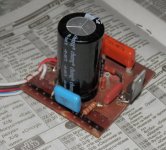
It might be worth trying a printed circuit board from datasheet. It is quite correct, though it is too big.
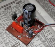
Or use a two-sided textolite. I've tried. This is very convenient, and there is absolutely no noise in the speakers without a signal at the input. I installed the output capacitor out of the board, and I didn't use separate PCB with capacitors for rectifier. The big cap on that PCB is the single cap for supply.
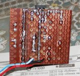
I know the view of the PCB is disgusting, but it was done just for experiment.
Or use a two-sided textolite. I've tried. This is very convenient, and there is absolutely no noise in the speakers without a signal at the input. I installed the output capacitor out of the board, and I didn't use separate PCB with capacitors for rectifier. The big cap on that PCB is the single cap for supply.
I know the view of the PCB is disgusting, but it was done just for experiment.
Attachments
Last edited:
- Status
- This old topic is closed. If you want to reopen this topic, contact a moderator using the "Report Post" button.
- Home
- Amplifiers
- Chip Amps
- LM1875 PCB Check