An op-amp is NOT a series of transistor amplifier stages put together, even thought it might be "reasonable" to conclude that.. It's more complex than that, and it's more than can be explained in a thread like this.
But there are voltage and current amplifiers in there. Just like discrete amps there are also current sources, current mirrors, etc etc.
Yes, this is all certainly true for modern op-amps that the the market currently demands, but I wasn't even thinking at that level of detail.You're right of course. And operational amplifier is a series of non-obvious sophisticated stages and elements composited in such a way as to achieve useful specifications to the engineers and designers that'll go on to utilize the thing once fabricated.
There are devices on board that are trivial to produce in silicon wafer (such as dual-emitter or more-emitter transistors, or intrinsically-thermally coupled current mirrors) that simply cannot be produced with discrete off-the-shelf elements. Is this a bug or a feature? Well… it turns out to be critical for the stable operation of op amps.
...
A 741 might be "useful" (amazingly, they're still made), but probably doesn't rely too heavily on such all-on-one-piece-of-silicon features.
Here's a discrete version of the 741:
https://cdn.evilmadscientist.com/KitInstrux/741/741_datasheet_revB.pdf
Yes, but it's still all very different from what I presume the OP was imagining or implying in post #10, three or more capacitively-coupled resistor-loaded common-emitter single-transistor gain stages, cascaded together to get high gain.But there are voltage and current amplifiers in there. Just like discrete amps there are also current sources, current mirrors, etc etc.
A knowledge of electronics is required to fully understand how it works. To ask this in another way, what happens to an input sine wave in each of the above stages? Maybe this can be described in a simpler way?
For the discrete 741 I see a push pull pair at the beginning stage, and a single transistor at the output / gain stage, is this correct? What's all this about difference amplification etc.
For the discrete 741 I see a push pull pair at the beginning stage, and a single transistor at the output / gain stage, is this correct? What's all this about difference amplification etc.
The 741 has a differential (or LTP, long tailed pair) input stage.
Differential amplifier - Wikipedia
There is a VAS or voltage amplifier stage marked as 'gain stage' on your diagram.
Finally there is a Class (A)B output stage.
----------------------------------------------------------------
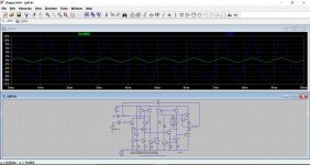
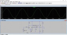
This is the 741 in simulation with a 1 volt sine wave applied. R11 and R12 set the gain.
Next is the input and output voltage. Can you see how the gain has been set by those resistors ?
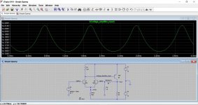
You asked what happens to a sine wave as goes through the amplifier. Well you might be in for a shock This shows the sine wave as it is applied to the gain stage at the base of Q16. As well as the obvious distorted look, also check out the amplitude at the left scale.
Differential amplifier - Wikipedia
There is a VAS or voltage amplifier stage marked as 'gain stage' on your diagram.
Finally there is a Class (A)B output stage.
----------------------------------------------------------------
This is the 741 in simulation with a 1 volt sine wave applied. R11 and R12 set the gain.
Next is the input and output voltage. Can you see how the gain has been set by those resistors ?
You asked what happens to a sine wave as goes through the amplifier. Well you might be in for a shock
This shows the sine wave as it is applied to the gain stage at the base of Q16. As well as the obvious distorted look, also check out the amplitude at the left scale.Attachments
It's a differential pair at the input Differential Transistor Amplifiers | Discrete Semiconductor Devices and Circuits Worksheets
That's still a little too advanced for me. If you imagine that each stage has two points where you can connect probes to as the input and output terminals, what will the oscilloscope show? I know the line levels I use are sine waves above and below zero voltage, for example driving headphones from a phone output jack. So the complete waveform is there.The 741 has a differential (or LTP, long tailed pair) input stage. <snip>
What does each stage do to the waveform? That will suffice for now.
See what you make of this.
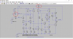
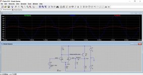
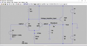
Here is a 3 transistor opamp that behaves just like a 741 or any other typical device.
The key building blocks are the differential input stage (Q1 and Q2) and the voltage amplifier stage Q3.
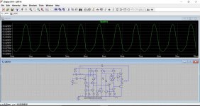
These are the key waveforms when a 1 volt peak sine is applied. In the second image the red and green traces overlay each other... but can you see why that is so ? The third image is the voltage applied to the 'VAS' or voltage amplifier stage. The fourth image is the voltage at the tail.
Within the opamp, the clean sine wave becomes unrecognisable as it enters the voltage amplifier stage. This is nothing more than a common emitter stage running in class A, and this stage on its own would have high voltage gain.
It is the action of wrapping the feedback loop around the opamp that now sets the all important gain.
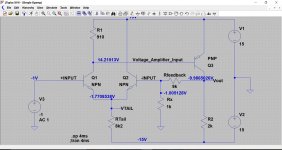
When the input is at 1 volt DC (for example... see last two images), and we will make it DC as its easier to understand, then the super high gain of the voltage amplifier wants to amplify that by a massive amount. Many thousands of times in reality.
What happens now is that the output feeds that voltage back into the - input of the opamp via the feedback network.
When the - input reaches the same level as the input voltage (which is applied to the + input) a state of balance is reached and the output settles to this new voltage.
In this example the feedback resistor network of 9k and 1k means that we need 10 volts on the output to deliver a 1 volt feedback voltage to the - input. Its just ohms law. The ratio of the feedback resistors set the gain. The last image shows -1 volt applied to the input.
(you really need to look at simple two stage amplifiers first, and understand how they work... which I think someone mentioned earlier)
Here is a 3 transistor opamp that behaves just like a 741 or any other typical device.
The key building blocks are the differential input stage (Q1 and Q2) and the voltage amplifier stage Q3.
These are the key waveforms when a 1 volt peak sine is applied. In the second image the red and green traces overlay each other... but can you see why that is so ? The third image is the voltage applied to the 'VAS' or voltage amplifier stage. The fourth image is the voltage at the tail.
Within the opamp, the clean sine wave becomes unrecognisable as it enters the voltage amplifier stage. This is nothing more than a common emitter stage running in class A, and this stage on its own would have high voltage gain.
It is the action of wrapping the feedback loop around the opamp that now sets the all important gain.
When the input is at 1 volt DC (for example... see last two images), and we will make it DC as its easier to understand, then the super high gain of the voltage amplifier wants to amplify that by a massive amount. Many thousands of times in reality.
What happens now is that the output feeds that voltage back into the - input of the opamp via the feedback network.
When the - input reaches the same level as the input voltage (which is applied to the + input) a state of balance is reached and the output settles to this new voltage.
In this example the feedback resistor network of 9k and 1k means that we need 10 volts on the output to deliver a 1 volt feedback voltage to the - input. Its just ohms law. The ratio of the feedback resistors set the gain. The last image shows -1 volt applied to the input.
(you really need to look at simple two stage amplifiers first, and understand how they work... which I think someone mentioned earlier)
Attachments
(you really need to look at simple two stage amplifiers first, and understand how they work... which I think someone mentioned earlier)
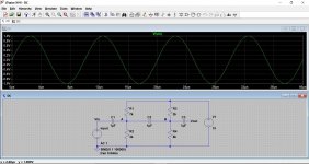
Ok so here is a video below, which explains the two stage amplifier. How accurate is it? And why on earth (no pun intended) should there be a residual volatile of 1.8 V after passing the capacitor? Also the oscilloscope has two probes, so I presume the other probe is always attached to the ground, although not shown.
YouTube
Its very accurate.
The capacitor does not allow DC to pass and so this allows the DC conditions of each stage to be set by the designer.
The capacitor then allows the stages to be coupled together as far as AC is concerned, but also prevents interaction at DC.
If you remove the capacitors, the DC voltages on each transistor will remain the same and you would still measure the same voltages the presenter of the video mentions.
The AC signal simply alters or 'modulates' the DC values.
So the 1.8 volts isn't a residual voltage left over by the cap, it is the voltage derived from the two resistors biasing the transistor and will be present whether or not the caps are fitted.
Last edited:
The final capacitor is able to remove all DC voltage?
Also, is this assumption correct?
It is a lot clearer now, but need to breadboard some stuff an experiment.
Also, is this assumption correct?
Also the oscilloscope has two probes, so I presume the other probe is always attached to the ground, although not shown.
It is a lot clearer now, but need to breadboard some stuff an experiment.
Oscilloscopes can have multiple channels, each of which have two wires, one of which is generally (but not always) connected to ground. There are differential probes, which show the difference between the two connections. Also you can “float” many modern oscilloscopes and connect the ground reference for the whole instrument to an AC or DC voltage. Finally you can do math between two channels, so for example you could do the difference between channel 1 and 2.
Haven’t you been down this road a couple of times already? Did you forget everything you learned?The final capacitor is able to remove all DC voltage?
Also, is this assumption correct?
It is a lot clearer now, but need to breadboard some stuff an experiment.
Understanding Transistor amplifier with an online simulation
 please note that starting multiple threads on the same/similar topics or asking the same questions repeatedly may be construed as trolling and is strictly against the Forum Rules.
The capacitor does allow DC to pass and so this allows the DC conditions of each stage to be set by the designer.
Typo on my part.
Should read:
The capacitor does not allow DC to pass
The final capacitor is able to remove all DC voltage?
Also, is this assumption correct?
It is a lot clearer now, but need to breadboard some stuff an experiment.
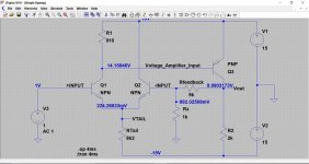
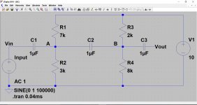
See if you can understand and work out how this works. The input is a 1 volt sine centred around zero volts.
What do you think you will see at points A, B and Vout ?
What is the DC voltage at those three points ?
What will happen to the AC signal at those points ?
Hint... the values and numbers make it easy to work out. No calculator required
Attachments
- Status
- This old topic is closed. If you want to reopen this topic, contact a moderator using the "Report Post" button.
- Home
- Amplifiers
- Chip Amps
- How really do chip amps work?