I know there are dozens (maybe hundreds) of amps designs with LM3886 here in this forum, but I'd really like to create my own layout by implementing some concepts that I have in my head.
So, I'm here to submit the design that I am developing for your comments.
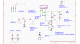
This is the diagram I created and calculated. I include the comments of my calculations for future reference. I apologize if I am copying any ideas from anyone, but I have actually studied many designs/concepts available on the internet. I do not even know who inspired me.

Undoubtedly ground is a deciding factor for a successful layout, so I paid special attention to that. Note in the diagram that we chose a system with two grounds. One for high current and one for low (signals).
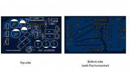
The layout of the PCB looks like this:

Note that I made slots in the ground plane in order to form a star ground. I'm still in doubt if I do the same for low current GND.
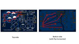
So the power and GND paths are these:

What do you think?
Feel free to comment and critique.
Note: I do not recommend anyone to copy this layout (yet) because it has not been tested and is in development.
So, I'm here to submit the design that I am developing for your comments.
This is the diagram I created and calculated. I include the comments of my calculations for future reference. I apologize if I am copying any ideas from anyone, but I have actually studied many designs/concepts available on the internet. I do not even know who inspired me.
Undoubtedly ground is a deciding factor for a successful layout, so I paid special attention to that. Note in the diagram that we chose a system with two grounds. One for high current and one for low (signals).
The layout of the PCB looks like this:
Note that I made slots in the ground plane in order to form a star ground. I'm still in doubt if I do the same for low current GND.
So the power and GND paths are these:
What do you think?
Feel free to comment and critique.
Note: I do not recommend anyone to copy this layout (yet) because it has not been tested and is in development.
Attachments
Last edited:
Those slots are doing more harm than good. The zobel ground has to return as quick as possible to the decoupling caps pins, not the power ground terminal. The ground of the mute cap is not critical. Delete at least the three top slots.
A thread to read from 1st page to last: LM3886 PCB vs Point-to-Point (with data)
A thread to read from 1st page to last: LM3886 PCB vs Point-to-Point (with data)
Tks.Those slots are doing more harm than good. The zobel ground has to return as quick as possible to the decoupling caps pins, not the power ground terminal. The ground of the mute cap is not critical. Delete at least the three top slots.
A thread to read from 1st page to last: LM3886 PCB vs Point-to-Point (with data)
Those slots are doing more harm than good. The zobel ground has to return as quick as possible to the decoupling caps pins, not the power ground terminal. The ground of the mute cap is not critical. Delete at least the three top slots.
A thread to read from 1st page to last: LM3886 PCB vs Point-to-Point (with data)
+
That thread should be sticky
And read this.
Those are MUST read
") .
.The whole point of GND plane is negated by those huge cuts. You need low impedance(not just resistance) ground. Sometimes cuts are unavoidable, but it is better to have smart layout if you can choose options.
Put Thiele on board. Ditch 680pF on input and put 220pF in between Vin+ and Vin-. Replace 100uF decouling caps with 22uF organic polymer and make sure 4.7uF are X7R.
Ditch the C12 and C13.
Connect the signal and power ground at output.
Measure feedback voltage at Thiele input.
You won't gain anything by "correcting" those resistance values with trim pots.
Best regards.
TKS.+
That thread should be sticky
And read this.
Those are MUST read
The whole point of GND plane is negated by those huge cuts. You need low impedance(not just resistance) ground. Sometimes cuts are unavoidable, but it is better to have smart layout if you can choose options.
Put Thiele on board. Ditch 680pF on input and put 220pF in between Vin+ and Vin-. Replace 100uF decouling caps with 22uF organic polymer and make sure 4.7uF are X7R.
Ditch the C12 and C13.
Connect the signal and power ground at output.
Measure feedback voltage at Thiele input.
You won't gain anything by "correcting" those resistance values with trim pots.
Best regards.
I found all the information I needed to know on this thread:
LM3886 PCB vs Point-to-Point (with data)
LM3886 PCB vs Point-to-Point (with data)
- Status
- This old topic is closed. If you want to reopen this topic, contact a moderator using the "Report Post" button.
- Home
- Amplifiers
- Chip Amps
- One more amp design with LM3886