I totally agree.
Feedback pole = 15.9 Hz
Input pole = 4.9 Hz
Perfect combination for distortion. It is the input pole that must always be the dominant pole, preferably by a factor of 10. This way the feedback capacitor has virtually no effect on the performance of the circuit.
C2= 100 uF moves the feedback pole down to 1.59 Hz. In practice this works fine with an input pole of 4.9 Hz, since both poles are low enough to be effectively unobtrusive.
With C2 so large, you want to add anti-latch up (clamp) diodes to C2.
I see so many circuits that ignore this basic principle. To me it's a no brainer.
Can you explain it more with the datasheet's schematic as an example?
Attachments
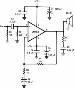
C2 >= Sqrt(2) * C1 * R2 / R3
That places C2 at >=68.4uF. Use 80uF, or 100uF.
I would go straight to 150uF, or 220uF.
Then add 4 signal diodes (1n4148 or 1n914) across the polarised electrolytic.
a series pair in one direction and a second series pair in the other direction.
This ensures that during abuse the capacitor is never exposed to more than 1.2V in either direction.
During normal use the capacitor has virtually zero AC voltage across it and just a few tens of DC milli-volts.
You can use as low as 6V polar, but possibly better to use 10V, or 16V
You have still not added RF input filter, nor the damped output inductor.
Last edited:
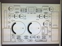
Hi, I have tried to create a schematic from the board. But it doesn't look right. Where is the input cap? Please take a look at this.
Attachments
Your schematic is going to lead you into making mistakes in how you lay out your traces.
1.) add an input cap in series with the input lead.
2.) add an input resistor in series with the input lead.
These two series components are each half of their respective filters.
the 680pF + 1k0 gives an RC low pass filter with F-3dB ~230kHz
the 51k + 1.8uF gives a CR high pass filter with an F-3dB ~1.7Hz
3.) connect 887r to input signal return and to 680pF and to 51k. DO NOT connect feedback to power ground. This group of input components and their traces MUST be laid out to minimise LOOP AREA.
4.) add a voltage reference link between signal return and speaker return. In this link leave 6pads for three parallel components: a resistor and two power diodes.
5.) change the upper NFB resistor to match the 51k input resistor.
or
Adopt DrE.Cherry and add his phase compensating network to the NFB. Now you would have three off 20k in the upper feedback and the input resistor gets changed to 60k to match and give low offset. or you could use three 18k or three 22k or etc.
6.) move the 0.1nF (HF decoupling) to be right next to the power pins. Once you have the package size selected for tolerable inductance, then find the biggest capacitance in that package. It might be 220nF, or 330nF.
Move the Power input to the INPUT side of the electrolytics (MF decoupling). The power MUST come in from one side and leave on the other side. It's the same for the HF decoupling.
7.) add in the damped inductor. It does not need to be on the PCB, but at least show it to remind you that it will be somewhere.
8.) connect the speaker return to the decoupling capacitors. Connect the Output Zobel to the decoupling capacitors. This reminds you that they form a current carrying circuit and YOU need to DESIGN that circuit with minimal LOOP AREA as you lay out the traces.
Why are you showing values from E96 and E192 ranges?
E24 is good enough for resistors and we can usually manage with E6 values for capacitors.
Last edited:
Your schematic is going to lead you into making mistakes in how you lay out your traces.
1.) add an input cap in series with the input lead.
2.) add an input resistor in series with the input lead.
These two series components are each half of their respective filters.
the 680pF + 1k0 gives an RC low pass filter with F-3dB ~230kHz
the 51k + 1.8uF gives a CR high pass filter with an F-3dB ~1.7Hz
3.) connect 887r to input signal return and to 680pF and to 51k. DO NOT connect feedback to power ground. This group of input components and their traces MUST be laid out to minimise LOOP AREA.
4.) add a voltage reference link between signal return and speaker return. In this link leave 6pads for three parallel components: a resistor and two power diodes.
5.) change the upper NFB resistor to match the 51k input resistor.
or
Adopt DrE.Cherry and add his phase compensating network to the NFB. Now you would have three off 20k in the upper feedback and the input resistor gets changed to 60k to match and give low offset. or you could use three 18k or three 22k or etc.
6.) move the 0.1nF (HF decoupling) to be right next to the power pins. Once you have the package size selected for tolerable inductance, then find the biggest capacitance in that package. It might be 220nF, or 330nF.
Move the Power input to the INPUT side of the electrolytics (MF decoupling). The power MUST come in from one side and leave on the other side. It's the same for the HF decoupling.
7.) add in the damped inductor. It does not need to be on the PCB, but at least show it to remind you that it will be somewhere.
8.) connect the speaker return to the decoupling capacitors. Connect the Output Zobel to the decoupling capacitors. This reminds you that they form a current carrying circuit and YOU need to DESIGN that circuit with minimal LOOP AREA as you lay out the traces.
Why are you showing values from E96 and E192 ranges?
E24 is good enough for resistors and we can usually manage with E6 values for capacitors.
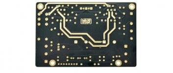
Thank you for you very detailed response. But this board or layout isn't mine. I have bought a board with all the components from AliExpress. The amp after assembly doing alright. No hiss, hum or anything. I haven't seen any instability. But I don't understand where is the input cap. Can you find it from the picture of the board I have posted above? If there is no input cap, I am planning to add a 1.5uf and also want to change the nfb cap to 100uf and resistor to 2.7k ohm, but if and only if my trace from the board is the right one. Thanks again.
Last edited:
looks like there is no DC blocking cap = mixed AC and DC coupling = BAD.
looks like there is no RF filter = interference from all the EMI emitting equipment in your home and your neighbours home = BAD.
Looks like the HF decoupling is too far from the power pins = no effective HF decoupling = BAD.
Don't waste any more time on that PCB. Bin it.
looks like there is no RF filter = interference from all the EMI emitting equipment in your home and your neighbours home = BAD.
Looks like the HF decoupling is too far from the power pins = no effective HF decoupling = BAD.
Don't waste any more time on that PCB. Bin it.
But the amp sounds very very nice. I just don't understand.
It was explained in excruciating detail to you. You have to pick poles that work, and don't stack them up. You do not want the dominant pole in the feedback network.
Commercial products contain these flawed circuits. They work fine or else they wouldn't be a "recommended application" circuit in the datasheet.
A 15.9 Hz pole is going to intrude on the audible band. Put that pole in the feedback network and it will produce distortion in the audible band.
If you're not going to build it right, why bother? Big box stores are full of cheap consumer products that contain these flawed circuits. And it literally took me less than two minutes with an engineering calculator to figure out how to correct the flaws, which tells me that the "designer" of these products is not an engineer at all.
.
Looks like the HF decoupling is too far from the power pins = no effective HF decoupling = BAD.
Another common mistake in consumer products. This leaves A LOT on the table.
Super easy to correct. Solder the decoupling caps directly to the chip pins on the bottom of the board. I always do this no matter what.
Don't waste any more time on that PCB. Bin it.
You could do better with veroboard.
15.9 Hz pole? That's not my board.It was explained in excruciating detail to you. You have to pick poles that work, and don't stack them up. You do not want the dominant pole in the feedback network.
Commercial products contain these flawed circuits. They work fine or else they wouldn't be a "recommended application" circuit in the datasheet.
A 15.9 Hz pole is going to intrude on the audible band. Put that pole in the feedback network and it will produce distortion in the audible band.
If you're not going to build it right, why bother? Big box stores are full of cheap consumer products that contain these flawed circuits. And it literally took me less than two minutes with an engineering calculator to figure out how to correct the flaws, which tells me that the "designer" of these products is not an engineer at all.
15.9 Hz pole? That's not my board.
I believe you're right. We were analyzing this circuit.
Andrew spelled it out for you. But I'll give you the highlights for this circuit.
R2 and C2 form a pole in the feedback network. That pole is 1/[2(pi)(R2)(C2)] =7.2 Hz. For your circuit with R2 = 887 ohms the pole is 8 Hz.
R1 and C1 form a pole in the input circuit. That pole is 3.3 Hz.
This is not as bad as the first circuit but still not right. Change C2 to 100 uF and the feedback pole is now 1.8 Hz. This makes the input pole dominant and is much better.
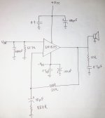
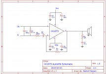
Schematic From the AudioMd Board of lm1875
Hi, I think I have successfully traced the board and created the schematic. I have attached it along with the datasheet's schematic. Now I have few questions.
1. As the modern sources like computer, mobile, cd player etc are dc decoupled generally, do I still need to add an input cap? As I have read that without input cap sound quality is better.
2. If I can omit the input cap, do I need that NFB cap? It seems this schematic has a CR filter on pin 2 instead of RC. What will be the consequences? Does it matter when there is no input cap?
3. From the datasheet's schematic, we can see there is no RF filter. Then why do we need to implement it as TI engineer has omitted it?
4. As I have read the value or R1 or R3 should be similar. If I add a volume pot of 50K, shouldn't it solve the problem more or less?
Thanks for bearing me.
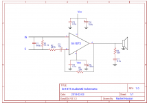
Attachments
1. As the modern sources like computer, mobile, cd player etc are dc decoupled generally, do I still need to add an input cap? As I have read that without input cap sound quality is better.
If you're driving it with a DC coupled source, then you absolutely need an input cap. As far as sound, the whole point of calculating poles is to ensure there is virtually no sonic intrusion introduced by the caps. Did you read my explanation of how much distortion a capacitor can introduce for a given input impedance? Read it again.
2. If I can omit the input cap, do I need that NFB cap? It seems this schematic has a CR filter on pin 2 instead of RC. What will be the consequences? Does it matter when there is no input cap
You absolutely cannot omit the feedback cap unless you use a servo. Omitting the cap will increase the DC gain and possibly (most likely) cause excessive DC offset, especially if you omit the input cap.
Again, the whole point of calculating poles, and figuring out how to arrange them in a given circuit, is to avoid intruding on the passband and also minimizing the distortion. I already explained it to you, with examples.
If you're driving it with a DC coupled source, then you absolutely need an input cap. As far as sound, the whole point of calculating poles is to ensure there is virtually no sonic intrusion introduced by the caps. Did you read my explanation of how much distortion a capacitor can introduce for a given input impedance?
I was talking about DC decoupled one.
Is 10uF cap on pin 2 acting as a NFB cap? And what will be the effect of a CR filter apparently there in the schematic?
2.)Hi, I think I have successfully traced the board and created the schematic. I have attached it along with the datasheet's schematic. Now I have few questions.
1. As the modern sources like computer, mobile, cd player etc are dc decoupled generally, do I still need to add an input cap? As I have read that without input cap sound quality is better.
2. If I can omit the input cap, do I need that NFB cap? It seems this schematic has a CR filter on pin 2 instead of RC. What will be the consequences? Does it matter when there is no input cap?
3. From the datasheet's schematic, we can see there is no RF filter. Then why do we need to implement it as TI engineer has omitted it?
4. As I have read the value or R1 or R3 should be similar. If I add a volume pot of 50K, shouldn't it solve the problem more or less?
Thanks for bearing me.
power amplifiers can be AC coupled or DC coupled (not decoupled- that's a term applied to supply rail decoupling).
Sometimes you get a stupid "designer" that uses mixed AC and DC coupling. I suggest you NEVER implement mixed.
AC coupled power amplifiers block DC at the input and this has the dual purpose of setting the low frequency response.
They also have a DC gain that is set to 1times (+0dB) and this is achieved with a DC blocking capacitor in the NFB lower leg.
You NEED both DC blocking caps. In a well designed power amplifier the resulting output offset will be near zero volts.
3.)
no RF attenuation filter : Because the Ti copy writer was being stupid.
4.)
Vol pot : place the vol pot where you can reach it easily. That will not be at the power amplifier at the back of each speaker.
There is a long interconnect between the vol pot and the power amplifier. Because of the capacitance of this long cable and the capacitance of the RF filter, the vol pot NEEDs a Buffer.
Now back to 1.)
protect your speaker/s by using an AC coupled amplifier.
Then you can use any or many sources irrespective of whether some or none have a DC blocking capacitor in the output lead.
However, the system does NOT NEED two series connected DC blocking capacitors. One will do the job. If you know you have two DC blocking capacitors in series in your system, then that does affect the performance. 1/Ceffective = 1/Cout + 1/Cin
Let's take an example where you have a power amplifier with a 22k Rin and a 4u7F MKT blocking capacitor. F-3dB of this high pass filter is 1.5Hz
Now add on a source that has a 470nF blocking capacitor.
Ceffective = 427nF and F-3dB becomes 17Hz
The two series connected DC blocking capacitors have rolled off your low bass !
A good alternative is to have TWO outputs for each Source channel. The DC blocked (= AC coupled) and a second socket that bypasses the capacitor (labelled DC coupled).
You, the system assembler, choose which output socket to use.
Last edited:
Still wrong. Output offset is high and varies with temperature.Correction: Mistakenly didn't change the value of R3. It's 20K.
Last edited:
A cap that acts as a filter in the passband will introduce distortion (Read D.Self).I was talking about DC decoupled one.
Is 10uF cap on pin 2 acting as a NFB cap? And what will be the effect of a CR filter apparently there in the schematic?
If you move the filtering effect to outside the passband, then much of this distortion is only on the audio near the roll-off frequency.
If you move the filter at least a decade away from the passband, then the distortion becomes negligible.
Except for electrolytic capacitors. They produce extra distortion when used as filters. They need at least an extra octave away from the passband (again D.Self spells this out in great detail)
You need to educate yourself. This is a DIY site. It's about time you did some of the work.
Last edited:
A cap that acts as a filter in the passband will introduce distortion (Read D.Self).
If you move the filtering effect to outside the passband, then much of this distortion is only on the audio near the roll-off frequency.
If you move the filter at least a decade away from the passband, then the distortion becomes negligible.
Except for electrolytic capacitors. They produce extra distortion when used as filters. They need at least an extra octave away from the passband (again D.Self spells this out in great detail)
Great explanation. This is one of the points I am trying to make. This is a fine point of design that is ignored in many commercial grade designs. Also many internet circuits make a mess of this. But if you're trying to reduce distortion, this is low hanging fruit.
I will also say that stacking the low frequency poles a decade apart is often impractical. However if you make the poles low enough, and make the input pole higher than the feedback pole, then a reasonable compromise can be made. I gave an example of this in my calculations.
You already got the circuit working, and you say it "sounds good." So why not try this simple, inexpensive, easy to implement, proven principle. It works!
Also, you are not ready for direct coupled circuits. I never even bother because a properly engineered capacitor coupled circuit is simpler and works just as well. I personally think that the whole anti capacitor paranoia is simply because people don't know how to use them. I can make a circuit to highlight and measure the distortion produced by an electrolytic capacitor; I can also design an amplifier circuit that greatly mitigates that distortion.
For peer reviewed, often cited, original research about use of capacitors, read Cyril Batemen's papers on choosing capacitors. He even has one devoted to audio circuits.
- Status
- This old topic is closed. If you want to reopen this topic, contact a moderator using the "Report Post" button.
- Home
- Amplifiers
- Chip Amps
- LM1875 or TDA7498 For good clean sound (Boards shown in the post)