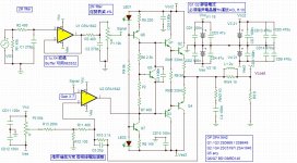
I design a tiny amp which provides around 16Vp-p output swing on 8 ohm load, which is also 16 watt, cute little amp for both headphone and bookshelf speakers.
The main configuration is class A op amp gain x7 push darlington current stage. DC couple with offset adj pot.
For reducing johnston noise I use 10k volume pot, followed by opa1642, which is excellent in common mode distortion, it will handle the input impedance change well while adjusting voulme. Darlington will make the load extremely light for the opa1642, so I can push the potential of open loop gain to limit, and might be able to keep the chip cool.
On gain stage with unbalanced current source, which will force opa1642 operate -3mA in class A mode. Power supply will be simple regulated 18V for op amp, unregulated power for darlington stage.
Output stage I wanted to find something around 3A, 2SA19xx series, but A1940 was the only one I can get from local distributor, Now I'm a bit concerned to hook headphone in this system.
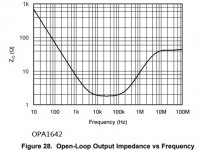
I'm concerning about stability issue, since opa1642 is rail to rail output, the output impedance varies, I don't know how will it interact with the capacitance between Vbe multiplier and in Bjt transistor. Also output transistor's BW is only 30Mhz, with 30mA quiescent current, it will be lower, I'm afraid it will create a second pole before close loop gain intersect with loop gain.
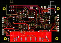
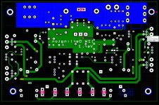
I've made PCB, some faults here and there. How bad will it be? that I didn't add 0.1uf decouple capacitor for current source.
What do you guys think about this cute 16 project?
The main configuration is class A op amp gain x7 push darlington current stage. DC couple with offset adj pot.
For reducing johnston noise I use 10k volume pot, followed by opa1642, which is excellent in common mode distortion, it will handle the input impedance change well while adjusting voulme. Darlington will make the load extremely light for the opa1642, so I can push the potential of open loop gain to limit, and might be able to keep the chip cool.
On gain stage with unbalanced current source, which will force opa1642 operate -3mA in class A mode. Power supply will be simple regulated 18V for op amp, unregulated power for darlington stage.
Output stage I wanted to find something around 3A, 2SA19xx series, but A1940 was the only one I can get from local distributor, Now I'm a bit concerned to hook headphone in this system.
I'm concerning about stability issue, since opa1642 is rail to rail output, the output impedance varies, I don't know how will it interact with the capacitance between Vbe multiplier and in Bjt transistor. Also output transistor's BW is only 30Mhz, with 30mA quiescent current, it will be lower, I'm afraid it will create a second pole before close loop gain intersect with loop gain.
I've made PCB, some faults here and there. How bad will it be? that I didn't add 0.1uf decouple capacitor for current source.
What do you guys think about this cute 16 project?
Attachments
Last edited:
cute 16watt, on the PCB I haven't decide how to connect different sections of GND yet. So everything is still scattering around.
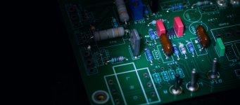
For installing output transistor, I'll screw Q1 2SD669A on top of Q2 2SC5197, ,Vbe multiplier in between 2 output transistor, in simulation when Q1, Q2 has same temperature, the quiescent current(working current?) will be more stable when temperature changes. Trouble is Q1 has Pc around 1W, but in simulation it will consume maximum 1.1W, so I hope Q2 can help and dissipate some heat.
For installing output transistor, I'll screw Q1 2SD669A on top of Q2 2SC5197, ,Vbe multiplier in between 2 output transistor, in simulation when Q1, Q2 has same temperature, the quiescent current(working current?) will be more stable when temperature changes. Trouble is Q1 has Pc around 1W, but in simulation it will consume maximum 1.1W, so I hope Q2 can help and dissipate some heat.
I design a tiny amp which provides around 16Vp-p output swing on 8 ohm load, which is also 16 watt
For 16V p-p into 8R, the power is ( 16 / 2x1.414 )^2 / 8 = 4W.
{snip}...opa1642 is rail to rail output, the output impedance varies, I don't know how will it interact with the capacitance between Vbe multiplier and in Bjt transistor. Also output transistor's BW is only 30Mhz ..... I didn't add 0.1uf decouple capacitor
You mean C3? That does not load the opamp at all.
The specified opamp is 11MHz gain-bandwidth, used at gain of 7. So closed-loop gain is 1.57MHz. The 30MHz output transistors, used as emitter followers, can be approximated as unity-gain to 30MHz, maybe 10MHz at low current. The output section does not appear to have a major 2nd pole inside the opamp's GBW.
The output transistors' hFE will fall with frequency, reducing the impedance seen by the opamp. At low frequency, 8r*100*100 or 80K, "no load at all". At 30MHz, 8r*1*1, heavy load. The opamp impedance is never as high as 1K. We need hFE*hFE> 120 to make 8r reflect as 1K. So hFE of 11 in each device. This is 2.7MHz, still well above where the opamp will go.
I have no doubt it "may" oscillate. Multi-stage amplifiers love to do that. Often not the circuit you designed, but the physical layout, including bypass caps at key points.
For 16V p-p into 8R, the power is ( 16 / 2x1.414 )^2 / 8 = 4W.
4W won't be cute, will be mini, you're sharp. I meant to say 32Vp-p. It's a good output power for bookshelf speakers. but for headphone, all I can say is , it's going to be powerful

to make 8r reflect as 1K. So hFE of 11 in each device. This is 2.7MHz, still well above where the opamp will go.
I have no doubt it "may" oscillate. Multi-stage amplifiers love to do that. Often not the circuit you designed, but the physical layout, including bypass caps at key points.
Thank you for the detailed reply, I've tried to find the answer for this kind of question in Chinese forum with no luck.You're a savior
I wrote in the schematic in mandarin, make sure ft>10*ACL BW. Guess it will be difficult to achieve.what do you mean make 8r reflect as 1K, this part I don't quite understand. so op amp will see load as equal impedance and get half of the voltage?
Since I worried about the phase margin stuff, So I don't have the balls to put base stopper. I guess it will be a good idea to put it before q1. how would you recommend to decouple the darlington transistors, one 0.1uf for both, or one each?
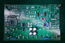
Done, it sounds pretty awesome. The photos I took was when I build it half way.
One small question, I adjust the output Iq 12mV, about 3x mA. After full loading 10mins, the measurement will be increased to 26mV, 8xmA, once stopped blasting, it will recover to 12mV in 1 min.
Is this okay heat stability?
One small question, I adjust the output Iq 12mV, about 3x mA. After full loading 10mins, the measurement will be increased to 26mV, 8xmA, once stopped blasting, it will recover to 12mV in 1 min.
Is this okay heat stability?
Attachments
Last edited:
Why did you set your RF filtering to F-3dB=1.5MHz?
I would drop that down two, or three octaves.
thankx, for both stage I will change it to around 400k ~ 250k hz, is that too aggressive? When the Pot is maximum I can hear some buzz on sensitive headphone, does that have anything to do with the low pass?
Many here use between 40kHz and 1MHz
But the consensus seems to be around 150kHz to 300kHz.
I use 160kHz (RC=1us) to 234kHz (RC=680us), or ~ one decade above 20kHz
400r + 270pF gives RC=108us
Thankx for the good idea. I replaced the buffer stage 270p to 1nF(from my stash), Done and Done. Originally I put 270pF bcs I don't want the dac output overshoot.
The result is pretty sweet, doesn't effect sound quality at all, and now hanging signal cable doesn't act like RF receiver. Why do you mention RC, normally I calculated it by f = 1 / 2piRC
the RC is built into your formula: F-3dB frequency = 1/ 2pi RC
using RC allows very quick comparison of filters.
It is common to use RC in many filters, rather than to refer to the frequency, eg. in FM tuners the time constant for the HF emphasis/de-emphasis is either 50us, or 75us, in tape recording and RIAA one sees RC time constants.
using RC allows very quick comparison of filters.
It is common to use RC in many filters, rather than to refer to the frequency, eg. in FM tuners the time constant for the HF emphasis/de-emphasis is either 50us, or 75us, in tape recording and RIAA one sees RC time constants.
Cute 16w is just moody
You're so right about this. If I don't connect the Zobel network to GND, turn the volume up, it will have 2 volt DC output, not very stable. and I put 5.1 ohm base stopper on the first stage bjt, even worse, on the 'right condition', it oscillate like no tomorrow.
I haven't solder the feedback capacitor yet.
Just with Zobel everything is fine.
What a moody amp.
I have no doubt it "may" oscillate. Multi-stage amplifiers love to do that. Often not the circuit you designed, but the physical layout, including bypass caps at key points.
You're so right about this. If I don't connect the Zobel network to GND, turn the volume up, it will have 2 volt DC output, not very stable. and I put 5.1 ohm base stopper on the first stage bjt, even worse, on the 'right condition', it oscillate like no tomorrow.
I haven't solder the feedback capacitor yet.
Just with Zobel everything is fine.
What a moody amp.
Oh well, it's not fine, it's a nasty demon. If I put laptop above the board and turn on a fan, it will oscillates if I turn the volume knob.
3 conditions have to meet to oscillate. I tame it with just Iron Core Bead thingy on the power supply input and it's fixed, no silent pops when I turn on fan or other stuff.
3 conditions have to meet to oscillate. I tame it with just Iron Core Bead thingy on the power supply input and it's fixed, no silent pops when I turn on fan or other stuff.
Many opamps use a supply range upto +-15Vdc, some go to +-18Vdc and a few go to +-22Vdc.
The maximum output voltage into a high impedance load is ~ 1/3rd (one third) of the rail to rail supply voltage.
If you use the boosted form of supply you can go much higher than that 1/3rd limit.
The maximum output voltage into a high impedance load is ~ 1/3rd (one third) of the rail to rail supply voltage.
If you use the boosted form of supply you can go much higher than that 1/3rd limit.
Many opamps use a supply range upto +-15Vdc, some go to +-18Vdc and a few go to +-22Vdc.
The maximum output voltage into a high impedance load is ~ 1/3rd (one third) of the rail to rail supply voltage.
If you use the boosted form of supply you can go much higher than that 1/3rd limit.
Interesting how you put everything. 1/3rd you mean like my op amp with +- 18V DC, the output is roughly +-17, so 34Vp-p/2.828 = 12Vrms roughly 1/3 DC voltage.
What about the boosted form of supply? can you recommend some configurations? Thank you sir.
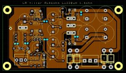
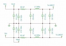
My power supply, 2200uF for Vcc2 , +pi filter to LM317.
It's a bit aggressive. and you guys are right,
hiss noise should be my least concern,
even hum is my least concern,
I try to install everything in a case .
The light Buzz I mentioned earlier, it was from the line power itself, it can be rejected by using line emi filter. And another buzz was caused by output channel way too near transformer.
But the real demon in the picture is ground loop from laptop to usb DAC to amp, when I try to connect the board to earth ground which I don't have in the house plugs, and notebook, every switching power supply shares the same extension plug. That was some nasty monster....
When I connect 10 ohm from signal GND to earth GND, it has 5xmV, then I try different resistors, about the same voltage. and when I measure the resistance between signal gnd and earth gnd on the 50 ohm resistor it shows like 110 ohm. Don't know why's that, doesn't look like ohms law.
I float the signal gnd for now with 2k resistor parallel 0.1uF + 2 diode back to back, don't know if it's a okay idea.
Attachments
- Status
- This old topic is closed. If you want to reopen this topic, contact a moderator using the "Report Post" button.
- Home
- Amplifiers
- Chip Amps
- Project Cute 16w