Hi,
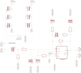
I've never designed a circuit schematic or layout before and decided to try putting together one for a LM3886 based chipamp as a learning exercise. I know that to get a working amp I'm best off just following the schematic in the datasheet but I thought I'd learn more by attempting a slightly modified design.
So far after trying to understand what I could from the datasheet and looking at examples from this site I've come up with the attached schematic.
If any of you are able to take a look and let me know whether I'm along the right lines I'd be grateful. I'm new to this (only downloaded Eagle yesterday) so I apologise if there are some basic errors in there.
I plan to use a 10k pot up stream of the signal input and the zobel network will be attached to the speaker outs so I've not included that here. Also I've left the power grounds and speaker/signal grounds separate here and plan to join them at the power supply caps - does that sound sensible? The supply will be 2x25V 300VA toroid and I'll be driving 8 ohm speakers.
Any thoughts/pointers will be gratefully received,
Thanks,
Simon.
Attachments
I suggest also to use a current limited power supply almost during first turn on. What I say is to put an incandescent (filament) lamp in series with one of the wires to the outlet, in the primary of the trafo. If anything goes wrong, this way you will protect a bit all set (Trafo, chip, speaker) and yourself.
Second, use a resistance of the same resistive value of the speaker, of sufficient power capability. Once again, if any goes wrong, it is cheaper a resistor than a speaker/cabinet.
I also suggest when the amp is finished, to add a small inductor shunted by a low value resistor (Usually a 10R 2W with some turns of wire winder over it) to difficult oscillations in the amp because of cable capacitances.
I suggest also to use a current limited power supply almost during first turn on.
Second, use a resistance of the same resistive value of the speaker, of sufficient power capability.
I also suggest when the amp is finished, to add a small inductor shunted by a low value resistor (Usually a 10R 2W with some turns of wire winder over it) to difficult oscillations in the amp because of cable capacitances.
Good advice. The Thiele network (L||R in series with the output) is shown in the data sheet for the LM3886. See Test Circuit #2 on page 5 of the data sheet.
You're missing the 220 pF from IN+ to IN- on the LM3886.
Tom
Perfect‼. In my case, I used TDA2006 chips, but similar in as behavior refers. I used 50µHy coils robbed fro PC SMPS (small tank with two pins downside), and shunted by a 10R 1R resistor. OK since about 1998 to the date.
Thanks for confirming.
Good advice. The Thiele network (L||R in series with the output) is shown in the data sheet for the LM3886. See Test Circuit #2 on page 5 of the data sheet.
You're missing the 220 pF from IN+ to IN- on the LM3886.
Tom
Doh... I'm adding that in right now - I'm on a steep learning curve. BTW great info on your website - I might understand it all one day! Thanks.
Also I've left the power grounds and speaker/signal grounds separate here and plan to join them at the power supply caps - does that sound sensible? .
It's good that you've left them separate, but connecting them at the power supply caps is not the best way. Have a look at this article by member Bonsai for the best way of connecting grounds to avoid loops http://hifisonix.com/wordpress/wp-c...re-up-a-Power-Amplifier_Updated-Autosaved.pdf
I like that you have separated the Signal ground from the Power ground.
There are some that I would do differently.
Speaker Return (SPKR-) goes to Power ground.
C4 goes to Power ground.
You will need to add a voltage reference between Signal return and speaker return so that the "amp" can work out what voltage it needs on the speaker output.
This extra voltage reference link can be a copper trace. It needs to meet the siganl return trace at a point and it needs to meet the speaker return trace at a point. Alternatively these two points can be linked by a low value resistor with a pair of inverse parallel diodes across it. This resistor will drop a few mVdc and leads to a small error in output offset. This can be corrected. The resistor also drops a few mVac and leads to a small error in output voltage. That why you need a low value resistor - to minimise the error.
All the Signal grounds are return routes for signal currents. The signal flow and signal return must be laid out to minimse the loop area in all of these input circuits.
The Power grounds are return routes for power currents. The power flow and power return must be laid out to minimse the loop area in all of these high current output circuits.
eg.
R1 is directly connected to INPUT-, show this as a wired connection. C2 is directly connected to INPUT-, show this as a wired connection. When you do this you can SEE the current loop and that prompts you to analysing the LOOP AREAs in those circuits.
Do similar for the power input currents . draw the connections as actual wires and then minimise the LOOP AREAS. Do the same for the output Zobel and agian for the speaker output.
It is the use of the gnd symbol rather than actual wires/traces that leads to errors in layout. I suggest you avoid the gnd symbol while you are still learning good layout.
And finally,
do not take any voltage references to the PSU smoothing capacitors.
Bring a three wire triplet (preferably a twisted triplet) from the PSU to the amplifier. One of these wires is the PSU zero volts. Anywhere along this wire or even on the trace after it enters the PCB can be used as the reference point that becomes the Main Audio Ground (MAG)
Last edited:
No !............. should I also move C5?
C5 is the NFB tapping into the signal return line. An alternative way of thinking about C5+R6 is that it is the -IN input. It connects to pin9, the VIN-. It is one of the differential inputs.
Again if you draw the sch without the gnd symbols and actually use wire/trace connections you will SEE the circuit.
You need to read about "how an opamp works".
What the 5pins need to see to allow an opamp to work.
Then compare those 5 opamp pins to a basic power amplifier circuit.
Look at Fig1 & Fig3.
They are drawn the same as one would for an opamp.
Last edited:
I have argued that we should "forget ground", but the advantages brought about by doing so have fallen on deaf ears.
"ground" is so ingrained in our thinking that most are not prepared to change.
I have used many unique and specific ground+ descriptor, but again few/none are willing to accept this less ambiguous way of posting technical information.
Quickly drawn schematics that use ground rather than wires/traces is just laziness.
"Ground" or "Chassis ground" is a terminology heritage from tube circuitry where elements were placed in a metallic chassis, and the vast majority of the times, also used for the PSU return, more or less how in cars. In AM radio receivers, with frequencies moderately low, it doesn't care if a solder to the chassis differs in 1 cm, but when TV sets appear, with IF of 50MHz, thing went complicated, and then, Engineers start to study the wright placement of the grounding points. Until a point in which there was punched in the chassis pieces of metal where the assemblers must do the soldering, say, starting from one of this things, passing through the tube socket (Heater, central shield, suppressor and returning 180° in other of this pieces. Then a complete shielding was done and a proper return to DC and Ac currents. Look how important this point was, that many european tubes (ECC84, EF183/4) had two cathode leads in the socket, one for input return and other for DC and output AC return.
In audio frequencies, if it is well known that frequencies are much lower, but currents are higher, sensitivities are higher, and then, a proper grounding is also very important. So, simply evaluate where high current paths flow (Rectifier, transformer(s), load) and where signal paths does (Input, return, NFB return, etc), and separate both as much as you can, avoiding overlapping them. Applying a good criterion, things will go good easily.
In audio frequencies, if it is well known that frequencies are much lower, but currents are higher, sensitivities are higher, and then, a proper grounding is also very important. So, simply evaluate where high current paths flow (Rectifier, transformer(s), load) and where signal paths does (Input, return, NFB return, etc), and separate both as much as you can, avoiding overlapping them. Applying a good criterion, things will go good easily.
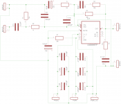
Okay... I've updated the schematic by including traces for all the grounds. I've included the 220pF across the inputs, a trace from Speaker- to V- and connected the Input- to 0V from the power supply. Does this look like an improvement?
If so then I guess the next step is to try and create a layout which keeps the signal/ground and power/ground loops separate and as closely looped as possible if that makes sense.
Here's the updated schematic:
If so then I guess the next step is to try and create a layout which keeps the signal/ground and power/ground loops separate and as closely looped as possible if that makes sense.
Here's the updated schematic:
Attachments

I got those from test circuit 2 in the data sheet... this is what it says; I just used the suggested values rather than trying to re-calculate.
10. Rf2
(1) At higher frequencies feedback resistance works with Cf
to provide lower AC Gain in conjunction with Rf1 and Ri. A high
frequency pole (lowpass roll-off) exists at:
fc = [Rf1 Rf2 (s + 1/Rf2Cf
)]/[(Rf1 + Rf2)(s + 1/Cf
(Rf1 + Rf2))]
11. Cf
(1) Compensation capacitor that works with Rf1 and Rf2 to reduce the AC Gain at higher frequencies.
- Status
- This old topic is closed. If you want to reopen this topic, contact a moderator using the "Report Post" button.
- Home
- Amplifiers
- Chip Amps
- Newbie LM3886 Circuit