tl072 would probably do the same job if the supplies suit.
http://www.ti.com/product/tl072
shows Ti's recommendations
http://www.ti.com/product/tl072
shows Ti's recommendations
Last edited:
Maybe, the 5532 has a low input impedance and swapping it for a circuit that uses high value resistors can cause problems. As a rough guide if the values in your circuit are a few K, likely given its a filter, you should be OK, if they are few hundred k then there may be problems.
My two penneth... the 5532 should be OK as long as you realise it will generate a measureable offset from the first stage, and that will carry through to stages 2 and 3. In itself that is no problem but make sure to measure the DC voltage across all the coupling caps and fit them to suit the offset polarity.
.
And you thought it would be simple.
It seems that your best bet by far would be, as AndrewT says, to use the TL072. It's the only certain direct plugin replacement.
Texas International states that the TL072 is simply the low-noise version of the TL082, which is obviously good for audio. Before the NE5532 came along the TL072 was highly regarded and much used in audio equipment. Even today there are people who prefer it.
You don't state your location, but the TL072 is widely available from Asian vendors on eBay at very low prices. Surely some of these must ship to your area?
.
Last edited:
Hi All,
Thanks for all of your advises. My location is Sri Lanka. As bentsnake mentioned, those IC are available at eBay at very low prices. But the issue is delivery time. However i'm going to order this from eBay.
Actually i'm not very expert in this subject. So i need all of you support to realize below my concerns.
Can you pls explain me the difference between JFET input and Bipolar input which is related to TL082 and NE5532?
If there any suggestion to change RC values of in put of my attached design where could be matched to NE5532 input? This is for, if i am going to complete the design with NE5532?
Can you pls tell me which could be the best Op amp (audio quality wise) among TL072, TL082, NE5532?
Can you pls explain me little bit about offset current and how to set it for a better out put? what are the coupling caps and how to fit them to suit to offset polarity?
Attachments

A Fet is voltage controlled.
A bipolar transistor is current controlled and the control input power of a bipolar transistor is 1/3 of the output power.
True about voltage / current control. I have no idea where you get the "1/3" figure from!
In any case, what has that to do with choosing a FET or BP opamp?? The main difference is input bias current - pA or nA, which is not relevant in the published circuit.
R1=R2=1K
C1=C2=470pF
If the impendance niveau left as it is, you should use a bipolar OP like NE5532.
Explain, please! As is, very unhelpful to a beginner.
Can you pls explain me the difference between JFET input and Bipolar input which is related to TL082 and NE5532?
Main differences... the TL072/82 use DIFET input stages which means that they have a very high input impedance (which can be useful for some circuits). Your circuit uses TL072/82 because they are a good audio performer at a good price.
The NE5532 draws more current than the TL072. That can be important when using a lot as the power requirements add up.
The NE5532 has significantly better ability to drive low impedance loads... but does that matter to you here ? Probably not.
Can you pls tell me which could be the best Op amp (audio quality wise) among TL072, TL082, NE5532?
You will be hard pushed to hear a difference between the TL072 and 5532. Both are extremely good. If you can get the TL072's and you can be sure they are genuine (not fakes) then I would probably recommend you use those.
Can you pls explain me little bit about offset current and how to set it for a better out put? what are the coupling caps and how to fit them to suit to offset polarity?
You can't alter the offsets in this design. They are what they are and depend on the opamps used. The TL072 will give much lower offset than the 5532 because the FET stage is immune to unbalanced impedances at the opamp inputs. The 5532 needs the circuit redesigning to give the lowest offsets.
Another reason to use the TL072.
what are the coupling caps and how to fit them to suit to offset polarity?
They are C3,C4 C9 and C10. Using the TL072/82 will give virtually zero volts offset. To measure the offset across the caps simply measure the DC voltage placing your red meter lead on the plus or positive end of the cap and the black lead on the minus or negative end. If the reading is a negative voltage (eg -20mv) then the cap needs fitting the other way around. That is more likely to be a problem with the 5532 which will generate DC offset. Those from the TL072 will be so low that you may not even be able to measure them.
input offset voltage and input offset current and input bias current are specified in the datasheets.
Output offset is not specified in the datasheets.
For a FET input opamp the output offset is very approximately the input offset voltage times the stage DC gain.
For a BJT input opamp the output offset is very approximately the difference in INput pin source resistance times the input offset current times the stage DC gain PLUS the input offset voltage times the stage DC gain.
If the output offset is not blocked, then the next stage sees that and applies it's own DC gain.
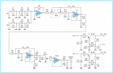
Using post13:
Considering US1A
input is DC blocked by C3 and C8 (far too big for audio signals)
+IN pin sees 47k||{47k+220k}||{47k+220k} ~ 34k76
-IN pin sees 0r
The difference is 34k76. For jFET this is ignored. For BJT this 34.76k is multiplied by the input offset current to give the first output offset term.
If I guess that input offset current is 50nA and input offset voltage is 1mV then output offset of US1A is {34k76*50nA + 1mV} * {47k/135k} ~ 1mV (pretty small even for the BJT)
Considering US1B
output offset = { 1mV + 50nA*(28k-1k3) + 1mV} * 11k5/10k ~4mV (still pretty low)
Considering US2A
output offset = { 4mV + 50nA*(122k/4+1k - 0) +1mV } * 22k/10k ~12mV (still low)
What you should do is look at the worst case datasheet values and decide whether every version of your circuit has acceptably low output offset.
If you are building one channel, just measure the output offset and see how much of your peak signal swing is wasted in overcoming the offset.
If anyone sees an error in the above please shout quickly so I can edit the procedure.
Output offset is not specified in the datasheets.
For a FET input opamp the output offset is very approximately the input offset voltage times the stage DC gain.
For a BJT input opamp the output offset is very approximately the difference in INput pin source resistance times the input offset current times the stage DC gain PLUS the input offset voltage times the stage DC gain.
If the output offset is not blocked, then the next stage sees that and applies it's own DC gain.
Using post13:
Considering US1A
input is DC blocked by C3 and C8 (far too big for audio signals)
+IN pin sees 47k||{47k+220k}||{47k+220k} ~ 34k76
-IN pin sees 0r
The difference is 34k76. For jFET this is ignored. For BJT this 34.76k is multiplied by the input offset current to give the first output offset term.
If I guess that input offset current is 50nA and input offset voltage is 1mV then output offset of US1A is {34k76*50nA + 1mV} * {47k/135k} ~ 1mV (pretty small even for the BJT)
Considering US1B
output offset = { 1mV + 50nA*(28k-1k3) + 1mV} * 11k5/10k ~4mV (still pretty low)
Considering US2A
output offset = { 4mV + 50nA*(122k/4+1k - 0) +1mV } * 22k/10k ~12mV (still low)
What you should do is look at the worst case datasheet values and decide whether every version of your circuit has acceptably low output offset.
If you are building one channel, just measure the output offset and see how much of your peak signal swing is wasted in overcoming the offset.
If anyone sees an error in the above please shout quickly so I can edit the procedure.
Last edited:
Back to C3 & C8
The DC blocking capacitors acts as High Pass Filters.
The F-3dB turn over frequency is given by the standard formula
F-3dB = 1 / {2 pi R C }
for R= 220k and C= 22uF you have F-3dB~ 0.03Hz
Change your 22uF to 1uF and adopt a plastic film type. At this new and still very low (F-3dB~0.7Hz) the added distortion of using an MKT type is going to be inaudible.
The RF attenuation filter is also very high. R=1k5, C=100pF RC = 150us
F-3dB ~1MHz. Reduce by a factor of 2 or even 5 to give an RC ~ 300us to 1us
- Status
- This old topic is closed. If you want to reopen this topic, contact a moderator using the "Report Post" button.
- Home
- Amplifiers
- Chip Amps
- Can I replace TL082 op amp with NE5532