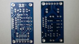
I have purchased this kit on ebay from China. I was interested because it didn't look like anything that is currently popular and it was using a choke and resistor paralleled in the output, much like the original circuitry shown in the old National Semiconductor spec sheet for an LM3886. Didn't cost much, figured I didn't have much to lose. It's the same kit mentioned in two other threads in this forum. Here recently and about a year ago here.
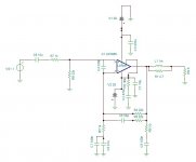
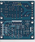
Being a cheap kit from China naturally means no schematic. So I took a look at the pc boards and drew one myself. Here are the pcb's and a schematic drawn on Tina-TI (first time using it, so there is still much to learn).
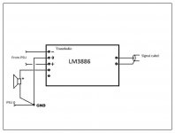
The schematic actually looks like it took a lot from the single supply circuit in the National or TI spec sheet but as a dual supply and changed some values to those used in the current iteration from ChipAmp.
I'm still in the planning stages for this project as I have a couple more underway, but any thoughts or recommendations would be appreciated.
Being a cheap kit from China naturally means no schematic. So I took a look at the pc boards and drew one myself. Here are the pcb's and a schematic drawn on Tina-TI (first time using it, so there is still much to learn).
The schematic actually looks like it took a lot from the single supply circuit in the National or TI spec sheet but as a dual supply and changed some values to those used in the current iteration from ChipAmp.
I'm still in the planning stages for this project as I have a couple more underway, but any thoughts or recommendations would be appreciated.
Attachments
And the questions are?
Although the actual PCB seems strange. There should be 100nF next to C3 and C2, near to the legs of the chip. And C2 and C3 is also in a strange place.
Sorry, late night, neglected to ask any questions. That schematic isn't exactly accurate. C2 should connect to the negative dc input on pin 4 and r2 should connect between pin 8 and c1. I'll redraw the schematic and label pins. What isn't shown in this version of the schematic is pin 7 to ground.
Also there is no value given for L1, the value shown was default for the software. I was given a about 27cm of magnet wire about 20 gauge. It's not the same value as in the datasheet. Anyone have an idea of what that should be? I guess I'll find out when I wind it and measure it.
Wait! What?! They sold you a PCB with no schematic and no instructions? And delivered a piece of magnet wire for the Thiele network inductor, but no instructions on how to wind it? Wow... That's the best eBay quality right there... ")
There are major improvements to be had by optimizing the power and ground routing of that board, but it's no worse than many of the other boards on eBay. Proper routing makes the difference between a stellar performer and a mediocre one - in particular in terms of THD above 1 kHz. I post measurements of the THD versus various layouts in the LM3886 P2P vs PCB thread.
The mute circuit isn't drawn correctly. I suggest retracing and posting a corrected schematic.
Now for the good news: The seller should receive plus points for including both the Thiele (L||R) and Zobel (R+C) networks. Many designers and builders omit those even though they are needed for stability. The seller also included the compensation networks (R+C across Rf and Cc across the inputs) to ensure the amp will work well near the supply rails. Plus points for that too!
The Thiele inductor needs to be around 1-2 uH. I suggest playing with this air core inductance calculator: Air Core Inductor Coil Inductance Calculator Set the length of the inductor to the distance between the two holes in the board intended for the inductor. Set the number of turns to a bit less than (length)/(wire diameter). Tweak the diameter in the calculator until you end up with 1-2 uH. Bigger is better, but if the inductance is too large, you start hurting the dampening factor at 20 kHz. Once you know the dimensions of the inductor, you can wind it by using the shank of a drill bit as a coil former.
~Tom
Last edited:
Thanks for the info Tom. Good to hear that of all the crappy stuff out there, this is less crappy. I knew there would be little to no instructions or a schematic going in.
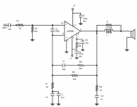
I redrew the schematic, including the mute circuit with different software. I had it as on the pcb in my pencil drawing but that didn't transfer over to the Tina-TI drawing that I posted. Here is a better drawing using more or less the component notation from the National datasheet.
I had a question on the mute circuit though, the value Rm is supposed to be determined with regard to the powersupply voltage so that the current on pin 8 is .5mA, so is this board built for +- 15vdc? Also I assume Cm is a delay?
I will re-read your LM3886 P2P vs PCB thread.
What improvements to power and ground optimizing should I consider on this layout? Jumpers, trace cuts? Or a thread that gives that information. I remember reading something on the matter in an XY board thread.
I knew there would be little to no instructions or a schematic going in. I redrew the schematic, including the mute circuit with different software. I had it as on the pcb in my pencil drawing but that didn't transfer over to the Tina-TI drawing that I posted. Here is a better drawing using more or less the component notation from the National datasheet.
I had a question on the mute circuit though, the value Rm is supposed to be determined with regard to the powersupply voltage so that the current on pin 8 is .5mA, so is this board built for +- 15vdc? Also I assume Cm is a delay?
I will re-read your LM3886 P2P vs PCB thread.
What improvements to power and ground optimizing should I consider on this layout? Jumpers, trace cuts? Or a thread that gives that information. I remember reading something on the matter in an XY board thread.
Attachments
Last edited:
When 500 uA is drawn on the mute pin, you can expect about 3 V on the mute pin. So the mute resistor can be calculated as: Rmute = (|VEE|-3)/500E-6.
Cmute provides some filtering as well as a little turn-on delay. I recommend 100 uF (as did National).
You'll get the best ground connection by using a ground plane as this provides the lowest inductance. It's a bit late to add a ground plane now... The only edit that may help the THD above 1 kHz is to run the feedback ground and input ground to the output connector ground directly. You can see my musings on that in the LM3886 P2P vs PCB thread I linked to earlier.
~Tom
Last edited:
I would use a 0.7uH parallel to 5r as the output feed after the Zobel.
0.7uH can be made from 7turns to 9Turns around an AA battery, using 1mm to 2mm enameled copper wire.
BTW, I agree with Tom, good on them for including the Thiele Network of R+C followed by L||R.
Many omit this and I consider that the National "optional" components a must for all beginners.
Another BTW,
Any Ebay seller who sells a "kit" without any customer support deserves the worst feedback the buyer can provide. A big -ve and a thrashing in the comment.
SUPER NS LM3886TF
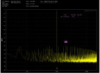
I have a pair of these to, running it on a very basic PS 2x36V, 4700uF filters, it delivers only 15W before clipping the the positive half period. After checking the PCB's I found a missing + PS link to the pin #5, after correcting it ,I got 55W out of it. A very decent amp, attached the 1kHz 3W 8 Ohm spectrum.
I have a pair of these to, running it on a very basic PS 2x36V, 4700uF filters, it delivers only 15W before clipping the the positive half period. After checking the PCB's I found a missing + PS link to the pin #5, after correcting it ,I got 55W out of it. A very decent amp, attached the 1kHz 3W 8 Ohm spectrum.
Attachments
Unfortunately there are many bad pcb to obtain on the Internet, this one may not be the worst.
I use this PCB self with some internal modifications (2x 0,1μF on the voltage at the chip and moving the feedback ground (capacitor-) to output ground.
tomchr writed "The only edit That apr help the THD above 1 kHz is to run the feedback input ground and ground to the output connector ground directly."
I attach a sketch of how I do the grounding.
The question is whether the shield of signal cable realy should be connected directly to the output connector instead of my sketch?
Maybe someone has comments?
Thank you in advance!
Attachments
tomchr writed "The only edit That apr help the THD above 1 kHz is to run the feedback input ground and ground to the output connector ground directly."
And I stand behind that.
I have measurements and simulations to back up that claim.I attach a sketch of how I do the grounding.
That actually makes the THD even worse as the ground impedance is increased.
I don't see any way to improve the performance of the PCB without a complete re-layout. I see several ways of making the performance worse, but that's rarely a goal.
Tom
Maybe someone has comments?
Having the input connector on the opposite side of the board from the output isn't good EMC practice. Ideally you'll want all connectors on one side of the PCB.
Reason being - your input ground will carry common-mode currents. Those will be flowing through the board with the sketched setup, inducing ground errors. If you keep the connectors on the same side, the ground currents won't flow across your PCB.
Thanks for clarifying and I hope it can be useful to others as well!
I've seen these excellent suggestions for grounding, but it becomes more unclear to me when the reality is seperate PCB’s and PSU.
Apart from not optimum layout on the PCB, do I understand it right so could the input wire shield advantageously be connected to a common GND point rather than output GND on the PCB?
What about common GND point and the chassi. Connection directly or via a resistor in parallel with capacitor?
Otherwise, these LM3886-amps are for the tweeters in my Linkwitz LXmini
- Status
- This old topic is closed. If you want to reopen this topic, contact a moderator using the "Report Post" button.
- Home
- Amplifiers
- Chip Amps
- Super NS LM3886 questions.