Though I am curious how one could clamp the LM3886 to let heat dissipate better.
See pictures by AudioLapDance above. I also suggest looking at ON-Semiconductor's app note: http://www.onsemi.com/pub_link/Collateral/AN1040-D.PDF
~Tom
You guys are so large haters that I don't have words to explain.
Will not share anything with you anymore … Will forget this forum …
Not all of us
") , I love your copper heat blocks!
, I love your copper heat blocks!Just connect the speaker directly to the amp.
good enough?
Attachments
I was looking at those, but could not understand why those would be considered special. I had envisioned having both sides of the LM3886 clamped by a heat sink so that there is more surface contact area with the heat sink.See pictures by AudioLapDance above. I also suggest looking at ON-Semiconductor's app note: http://www.onsemi.com/pub_link/Collateral/AN1040-D.PDF
~Tom
I was looking at those, but could not understand why those would be considered special. I had envisioned having both sides of the LM3886 clamped by a heat sink so that there is more surface contact area with the heat sink.
If you clamp all sides of the IC and have good thermal contact on all sides, the thermal system will consist of two thermal resistances in parallel. One thermal resistance will be that of the IC die to the heat sink through the DAP (that metal back side of the IC package). The other thermal resistance will be from the die through the plastic, the clamping block, to the heat sink. Do we agree so far?
Now, the total thermal resistance of these two thermal resistances in parallel follows the same math as electrical resistors in parallel. I.e. Rtotal = R1R2/(R1+R2). If one resistance is significantly smaller than the other, the total resistance will be approximately equal to the smallest of the two resistances. This is fundamental physics.
Now, back to the thermal system in question. The DAP is made of a material with very low thermal resistance. Therefore, the thermal resistance from the die through the DAP to the heat sink will be very low (assuming a good thermal interface between the heat sink and the DAP). The thermal resistance through the plastic is significantly higher than that through the DAP. It's probably several orders of magnitude higher. After all, electrical insulators tend to be good thermal insulators as well. Therefore, the total thermal resistance is overwhelmingly dominated by the thermal resistance through the DAP.
Even if you somehow managed to build a clamping device with good thermal contact on all sides of the IC, it would make only a negligible difference at best. Obtaining this negligible difference would require precision machining of each clamping block to fit each individual IC package to ensure a press fit on each IC. So hours of machining for no benefit. From an engineering perspective, that's a non-starter.
A clamping bar across the IC package as shown in Rowland's amp (pictures by AudioLapDance a few posts back) does make some amount of sense. The clamping bar ensures that the clamping pressure is distributed evenly across the DAP, which minimizes the thermal resistance from the die through the DAP to the heat sink.
~Tom
Some packages can be cooled from both sides :
IRF6718L2TRPBF International Rectifier | IRF6718L2TRPBFTR-ND | DigiKey
In this case, the top side is metal (not resin as LM3886), and the bottom is connected to thermal vias and perhaps a heat sink on the other side of the pcb (or just the ground plane)...
IRF6718L2TRPBF International Rectifier | IRF6718L2TRPBFTR-ND | DigiKey
In this case, the top side is metal (not resin as LM3886), and the bottom is connected to thermal vias and perhaps a heat sink on the other side of the pcb (or just the ground plane)...
Some packages can be cooled from both sides :
Yes some can, but if you look at the thread title you might note we are looking at one specific package here...
Music vs test tones
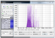
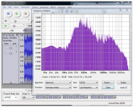
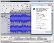
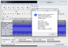
Tom, you had a discussion with BrianL earlier regarding the AP test tones. I was curious about this because I felt that Brian had a point. I have analyzed the test tones, and I now understand your point. The average signal of the AP signal is in fact pretty close to a music signal. I compared it to a pretty intense music signal from "Tool" (The pot) and they are both at roughly the same RMS level. See pictures of both RMS analysis and FFT. I will use the same signal for my future testing as well. Thank you for the tip.
Regarding the discussion about clamping I agree with the sensible way of doing it. Clamping like in the Rowland amp. There must be so little gain from extracting heat through the wrong side of the chip that it is just not worth the hassle.
A better option is to clamp a T-package directly to a thick 2"x 2" copper heat-spreader with just thermal paste and then electrically isolate that heat-spreader from the heat sink with a thermal pads.
Armand
Attachments
The type of clamping Jeff Rowland's amp uses is quit common. I was wondering about the mentioned "new method".If you clamp all sides of the IC and have good thermal contact on all sides, the thermal system will consist of two thermal resistances in parallel. One thermal resistance will be that of the IC die to the heat sink through the DAP (that metal back side of the IC package). The other thermal resistance will be from the die through the plastic, the clamping block, to the heat sink. Do we agree so far?
Now, the total thermal resistance of these two thermal resistances in parallel follows the same math as electrical resistors in parallel. I.e. Rtotal = R1R2/(R1+R2). If one resistance is significantly smaller than the other, the total resistance will be approximately equal to the smallest of the two resistances. This is fundamental physics.
Now, back to the thermal system in question. The DAP is made of a material with very low thermal resistance. Therefore, the thermal resistance from the die through the DAP to the heat sink will be very low (assuming a good thermal interface between the heat sink and the DAP). The thermal resistance through the plastic is significantly higher than that through the DAP. It's probably several orders of magnitude higher. After all, electrical insulators tend to be good thermal insulators as well. Therefore, the total thermal resistance is overwhelmingly dominated by the thermal resistance through the DAP.
Even if you somehow managed to build a clamping device with good thermal contact on all sides of the IC, it would make only a negligible difference at best. Obtaining this negligible difference would require precision machining of each clamping block to fit each individual IC package to ensure a press fit on each IC. So hours of machining for no benefit. From an engineering perspective, that's a non-starter.
A clamping bar across the IC package as shown in Rowland's amp (pictures by AudioLapDance a few posts back) does make some amount of sense. The clamping bar ensures that the clamping pressure is distributed evenly across the DAP, which minimizes the thermal resistance from the die through the DAP to the heat sink.
~Tom
Clampimg both sides of the same material to increase heat dissipation capability is common sense, at least since as long as I can remember. The main issue is the mechanism for making contact on both sides, of the metal tabbed LM3886 for example, to have equally good contact without creating significant differences in thermal resistance to the main conducting body or the dissipation fins.
Regarding the discussion about clamping I agree with the sensible way of doing it. Clamping like in the Rowland amp. There must be so little gain from extracting heat through the wrong side of the chip that it is just not worth the hassle.
I agree.
A better option is to clamp a T-package directly to a thick 2"x 2" copper heat-spreader with just thermal paste and then electrically isolate that heat-spreader from the heat sink with a thermal pads.
That would be another approach. Whether it'd be better than the T-package with a thermal pad by itself would depend on the clamping pressure, surface area, etc.
The type of clamping Jeff Rowland's amp uses is quit common. I was wondering about the mentioned "new method".
Please read Post #125. The thermal system I describe in that post is the "new method". The "new method" fails to provide any benefit as I describe in Post #125.
Clampimg both sides of the same material to increase heat dissipation capability is common sense, at least since as long as I can remember.
No it does not. The thickness of the mold compound between the DAP and the back of the TF package has to be very thin in order to minimize the thermal resistance. This is why there is only a difference of about 1 ºK/W between the T and the TF packages. The mold compound on the front of the package is much thicker, hence, provides much, much higher thermal resistance. Hence, the total thermal resistance, even when clamped using this "new method", is dominated by the thermal resistance through the back of the package. This is exactly what I describe in Post #125.
Think about it. 99.9999999 % (if not more) of the heat is conducted through the back of the package. Is it really worth the last 0.0000001 % to machine a precision clamp gizmo? I don't think so. That, to me, is common sense.
Now, had the IC package been symmetrical with a DAP and equivalent mold compound thickness on both sides of the die, you'd been correct. However, that is not the case.
~Tom
Last edited:
About the test tones, I havel always wonder what type of music they really equate to, or whether it is some kind of average?Tom, you had a discussion with BrianL earlier regarding the AP test tones. I was curious about this because I felt that Brian had a point. I have analyzed the test tones, and I now understand your point. The average signal of the AP signal is in fact pretty close to a music signal. I compared it to a pretty intense music signal from "Tool" (The pot) and they are both at roughly the same RMS level. See pictures of both RMS analysis and FFT. I will use the same signal for my future testing as well. Thank you for the tip.
Regarding the discussion about clamping I agree with the sensible way of doing it. Clamping like in the Rowland amp. There must be so little gain from extracting heat through the wrong side of the chip that it is just not worth the hassle.
A better option is to clamp a T-package directly to a thick 2"x 2" copper heat-spreader with just thermal paste and then electrically isolate that heat-spreader from the heat sink with a thermal pads.
Armand
In one situation while playing around with the MyRef, I forgot to put the isolator in, did hear a difference in sound, so I think proposing to copper heat spreader to the T package is an interesting one.
About the test tones, I havel always wonder what type of music they really equate to, or whether it is some kind of average?
In one situation while playing around with the MyRef, I forgot to put the isolator in, did hear a difference in sound, so I think proposing to copper heat spreader to the T package is an interesting one.
If you had a T-package without isolator you should have heard 'fzzt' as something blew unless you purposefully insulated your heatsink from the rest of the world.
I thought we were talking about the T package like used in the Rowland amp pic, why jump to picking on the TF package? I agree there is not much you can do more with a TF package.I agree.
That would be another approach. Whether it'd be better than the T-package with a thermal pad by itself would depend on the clamping pressure, surface area, etc.
Please read Post #125. The thermal system I describe in that post is the "new method". The "new method" fails to provide any benefit as I describe in Post #125.
No it does not. The thickness of the mold compound between the DAP and the back of the TF package has to be very thin in order to minimize the thermal resistance. This is why there is only a difference of about 1 ºK/W between the T and the TF packages. The mold compound on the front of the package is much thicker, hence, provides much, much higher thermal resistance. Hence, the total thermal resistance, even when clamped using this "new method", is dominated by the thermal resistance through the back of the package. This is exactly what I describe in Post #125.
Think about it. 99.9999999 % (if not more) of the heat is conducted through the back of the package. Is it really worth the last 0.0000001 % to machine a precision clamp gizmo? I don't think so. That, to me, is common sense.
Now, had the IC package been symmetrical with a DAP and equivalent mold compound thickness on both sides of the die, you'd been correct. However, that is not the case.
~Tom
The type of clamping that the Jeff Rowland amp uses actually avoids hole alignment issues during assembly.
Last edited:
Yes some can, but if you look at the thread title you might note we are looking at one specific package here...
Yeah, that was the idea...
@tomchr
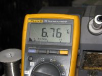
if lm3886 can output 6,7v at 50hz continous sine(not that averaged thing of yours), to speaker of 4 ohms ,without turning on spike and running at that output for full hour from +-12v psu, could you calculate how much heat is being transfered from chip to heatsink of dimensions 94mm *72mm *3mm , that same heatsink being mounted on front side of lm , and somehow prove to me and everyone else that it is worthless as you say it is.
as i am feeling good today i would like to propose a test,if you would like i will mount lm facing front to some huge heatsink i have available(better say water cooling with 240mm radiator) and connect it on better power supply to try to pull more power out of front side of chip than your comercial design can pull out of back of lm (but not "with vanishingly low THD and phenomenal sound quality" just as far as it goes without spike.).but that will i do only if you would be nice and actualy try this you call "new" mounting method for yourself and maybe measure whatever you measure to feel fine.
Last edited:
I think actually its only you. The rest of us understand that the metal tab is the thing you bolt down. Assuming you mean 6.7V peak sine wave that's a Gnats under 6W. The curves for the chip don't go down that low but we can extrapolate and its around 6W dissipation. Most normal applications would be around 30-50W. So I could believe that tab in free air and a small leakage to package side could handle 6W continuous.
The physics say there are easier ways to get an undetectable increase in volume out your circuit.
The physics say there are easier ways to get an undetectable increase in volume out your circuit.
I think actually its only you. The rest of us understand that the metal tab is the thing you bolt down. Assuming you mean 6.7V peak sine wave that's a Gnats under 6W. The curves for the chip don't go down that low but we can extrapolate and its around 6W dissipation. Most normal applications would be around 30-50W. So I could believe that tab in free air and a small leakage to package side could handle 6W continuous.
The physics say there are easier ways to get an undetectable increase in volume out your circuit.
i dont understand physics and what they say but this small heatsink of mine got hot so what physics say about that, and it was 6,7v measured with true rms meter if that makes difference?
and funny thing ,user who posted this method actualy used this in working amp with backside heatsink also connected.
i used only front to see how much i can get out of front side .
and if you look at picture that user posted you can see that they used TF version which everyone says have higher resistance case to heatsink , and maybe got to similar overall heat transfer with TF package as others get with T package, by just using this rather simple method of clamping.
That much is very clear.i dont understand physics and what they say .
That much is very clear.
you do realise you livin in 21st century and you livin in kingdom?i dont care about your opinion and neither you should about mine.
we here for data which i am trying to provide somehow but i cant as i dont know how.
if you know how then help.
when you do know physics like everyone seems to know on this forum , could you please make it clear to me how could i calculate how much dissipation there realy is from front side of chip ,could i use some ntc thermistors for temp measurments and how to translate resistance change to degrees change. and how to get some actualy real measurments out of that all. i dont care if in end it equals to 1w dissipation out of front side but i want to test it .
Last edited:
- Status
- This old topic is closed. If you want to reopen this topic, contact a moderator using the "Report Post" button.
- Home
- Amplifiers
- Chip Amps
- LM3886 Thermal Experiment (with data)