The old 555 has a supposed capability to source and sink up to 200mA, or more, but in practice the output drops significantly with load.
For example powering the ICM7555 or SE555 with 10V and drawing about 20mA results in 7.44V at the output, whereas at 1mA gives 9.84V at the output.
Is there a simple way to provide some sort of a buffer to give us say 50mA source and sink without any voltage drop issues?
I have been working on a full NPN push-pull stage on the simulator, three transistors in total, but if you have some better ideas please let me know.
What are you trying to drive?
I have found that a simple npn/pnp push pull stage works the best.
I used it for driving single FET's directly and I used it to drive a Gate transformer for use in a FET Class B stages.
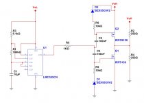
Here is my implementation,
http://www.diyaudio.com/forums/plan...tor-insulation-mylar-coating.html#post2531218
FWIW
jer")
I have found that a simple npn/pnp push pull stage works the best.
I used it for driving single FET's directly and I used it to drive a Gate transformer for use in a FET Class B stages.
Here is my implementation,
http://www.diyaudio.com/forums/plan...tor-insulation-mylar-coating.html#post2531218
FWIW
jer
Attachments
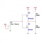
How about a simple N and P channel FET pair such as IRF240 and 9240. No resistors needed, just the two transistors.
That has worked better than ever imagined. I used what I had in the draw, so IRF9540 (P-channel) at the top and PSMN017-80PS (N-channel) at the bottom, switching happily from rail to rail with 0 load on the 555.
What are you trying to drive?
I have found that a simple npn/pnp push pull stage works the best.
I used it for driving single FET's directly and I used it to drive a Gate transformer for use in a FET Class B stages.
Here is my implementation,
http://www.diyaudio.com/forums/plan...tor-insulation-mylar-coating.html#post2531218
FWIW
jer
I need a level shifter and a current buffer. What I had overlooked was that with the buffer the requirements on the 555 would be minimal and thus the amount of level shifting needed would also be minimal. So maybe I do not need a level shifter, just a buffer. Anyway I just tried the MOSFETs and they switch from rail to rail, no need to use transistors.
This makes the output 180 out with gain. May not be a real problem for your application, but, may want to look out for ringing or other signs of instability.
Yes it is 180 degrees out but achieves rail-to-rail at 20mA and it looked ok on the scope there is some bouncing but I am using very large MOSFETs because I do not have small ones. Because of the smaller current requirements on the output of the 555 now that I have a buffer, I can also use a traditional NPN/PNP push pull, with one only resistor, which however loses around 700mV from either side of the signal. The MOSFETs follow the rails but the transistors follow the driving signal. I will try with smaller MOSFETs like the BS170 and something else.
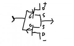
No, it is like this
OK. It is a valid configuration on low supplies. At higher voltage the Vgs rating of the FET's would be exceeded.
OK. It is a valid configuration on low supplies. At higher voltage the Vgs rating of the FET's would be exceeded.
From what I understand, you cannot place a N-channel MOSFET at the positive side and expect it to open fully. In that situation the Source would be at the same level as the Drain. The Gate then would need to be 3-4V higher than both Source and Drain, and where would that come from. So you are forced to use a P-Channel in that position. In my case it is even worse as the Gate driver is expected to be below the rail to start with.
This makes the output 180 out with gain. May not be a real problem for your application, but, may want to look out for ringing or other signs of instability.
I have received a bunch of IRFD120 and IRFD9120 - these are 100V/1A MOSFETs in a 4 pin DIP package.
I have used them in the circuit and they more or less behave like their much bigger brothers eg the 80V/50A PSMN017-80PS and the 100V/23A IRF9540.
What that means is that there is a bit of ringing on the transitions. They are also quite slow, much slower than a pair of transistors.
So I have added a speed-up capacitor, and a resistor to ground and the ringing has gone, plus the speed is now quite good.
Attachments
Beware of the shoot-through current spike caused by cross-conduction with this scheme: it could very well disturb other parts of your circuits if you don't take care.
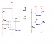
If AC-coupled is good enough for you, this circuit has no shoot-through to speak of and robust H and L states (and it does voltage translation, not only for Vcc, but also for GND or Vee if required):
If AC-coupled is good enough for you, this circuit has no shoot-through to speak of and robust H and L states (and it does voltage translation, not only for Vcc, but also for GND or Vee if required):
Attachments
Beware of the shoot-through current spike caused by cross-conduction with this scheme: it could very well disturb other parts of your circuits if you don't take care.
If AC-coupled is good enough for you, this circuit has no shoot-through to speak of and robust H and L states (and it does voltage translation, not only for Vcc, but also for GND or Vee if required):
Thank you Elvee. I was aware of this circuit when you offered it in an older discussion about switching capacitors. I have spent some time analysing this circuit and its magic, because it is magic. The problem this circuit tries to solve is to separate the biasing on the bases of the two transistors so they have the minimum overlap and thus the minimum cross conduction. I will try to see if something similar can be done with the FETs.
The first schematic seems to fix the cross conductivity but requires a lot of parts. The second schematic does more or less a good compromise with a 10R resistor to limit the current during all periods and during cross conduction of course. I monitored the power line on the scope and the presence of the 10R resistor fixes any noise / spikes. The 10nF capacitor really improves the speed of the FETs.
The 250R resistors are indicative of double the expected loads (so we have room for more).
We lose about 150mV due to the 10R resistor on the high side, I could have two 5R resistors to split the loss during the highs and lows but whatever...
The 250R resistors are indicative of double the expected loads (so we have room for more).
We lose about 150mV due to the 10R resistor on the high side, I could have two 5R resistors to split the loss during the highs and lows but whatever...
Attachments
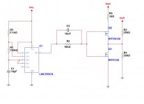
Why do you stick to the MOSfets, when the BJT's are more than capable to drive your load, and they work so much better? (and they are cheaper too).The first schematic seems to fix the cross conductivity but requires a lot of parts. The second schematic does more or less a good compromise with a 10R resistor to limit the current during all periods and during cross conduction of course. I monitored the power line on the scope and the presence of the 10R resistor fixes any noise / spikes. The 10nF capacitor really improves the speed of the FETs.
The 250R resistors are indicative of double the expected loads (so we have room for more).
Using modern, low capacitance and low threshold MOS, you can arrive at the same level as the Bjt's, but with traditional types, it is an uphill struggle.
I had proposed another solution, based on integrated MOS: the low side driver.
That frees you of all the constraints
- Status
- This old topic is closed. If you want to reopen this topic, contact a moderator using the "Report Post" button.
- Home
- Amplifiers
- Chip Amps
- 555 buffering