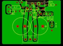
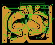
This is my second attemp of PCB design for LM3875 Gainclone . The design is very perliminary . finally , it will be able to accept various coupling caps or resistors size .
I filled up un-used area as common ground and implement the ground star concept . Components to IC distance kept to minimal .
Pin 2, 5, 9 have to be removed from IC to avoid short circuit .
BTW, I have a question about ouput of film using software ExpressPCB ? How can you print film without grid dots ? I made them in-visible in display . Is it restriction for freeware ?
Attachments
nice one ")
is it made with express PCB? you could double up top and bottom for the higher current lines, that is unless you are just using their program to make your own boards anyhow. I can not see anything wrong with it but i am no expert.
would you mind posting the file?
as for printing it is a bit bogus like that as far as i can see, if your monitor is large enough you could try this, since it is a small board.
in the options dialog, uncheck grid, silk screen, and top layer.
in the colors tab change it to white background and bottom layer black (or the other way around depending on how you make boards)
blow it up so it takes up as much of your screen as possible.
press print screen
open photoshop or whatever image program you have.
file > new (image size should default to size of your screen because you have it in your clipboard)
press ctrl - v
now the hard part.
you have to use photoshop or something to re-scale it back to the original size. i would just make copies and resize it a few times, print and see which one matches the lm3875 properly.
important thing is do not resize the original and then resize it again because it will be all pixelated, so save it first and then "save as" the resized versions
(trial and error) it is not the best way to do it because it is not super accurate, but for a small circuit like that nobody will know
is it made with express PCB? you could double up top and bottom for the higher current lines, that is unless you are just using their program to make your own boards
anyhow. I can not see anything wrong with it but i am no expert.would you mind posting the file?
as for printing it is a bit bogus like that as far as i can see, if your monitor is large enough you could try this, since it is a small board.
in the options dialog, uncheck grid, silk screen, and top layer.
in the colors tab change it to white background and bottom layer black (or the other way around depending on how you make boards)
blow it up so it takes up as much of your screen as possible.
press print screen
open photoshop or whatever image program you have.
file > new (image size should default to size of your screen because you have it in your clipboard)
press ctrl - v
now the hard part.
you have to use photoshop or something to re-scale it back to the original size. i would just make copies and resize it a few times, print and see which one matches the lm3875 properly.
important thing is do not resize the original and then resize it again because it will be all pixelated, so save it first and then "save as" the resized versions
(trial and error) it is not the best way to do it because it is not super accurate, but for a small circuit like that nobody will know
Hi,
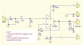
It is not really a good idea to use ground planes on power amplifers. The stray capacitance involved can cause instability and in power amplifers you need to define where the low frequency currents will flow.
For example in your circuit the charging currents from decoupling caps share the same path back to the "star" as the feedback resistor and the input resistor. This is not a good idea.
I would recomend looking through the archives for threads on layout as the implemetation of star grounding has been well covered.
Andy.
Some inspiration:
http://home.ca.inter.net/~cfraser/int1a.jpg
http://home.ca.inter.net/~cfraser/int2a.jpg
Ciao,
Fedde
http://home.ca.inter.net/~cfraser/int1a.jpg
http://home.ca.inter.net/~cfraser/int2a.jpg
Ciao,
Fedde
Ok i can do that, i can swap em with the space for the 1uf (which probably will not be needed anyways,
Just an update on printing from ExpressPCB, i got it to work exactly the right size first go.
1: do a print screen of it in black and white (see post 3 in thread)
2: find out the dimensions of the board by placing the mouse over the bottom right edge square, and write down te co-ordinates
3: (photoshop instructions other program will be different)
create a new document in photoshop and press "ctrl v" to paste your screen shot
4: crop exactly to the same size as the board edges.
4.5 oh doh..i forgot a step. when you first import it you can use the image > adjustments > brightness/contrast and max it out to get rid of the dots where the corners of traces are.
now to get rid of ugly jaggies
5: resize it 400%
6: use the magic wand to select the white area, then in the select menu "select similar"
7: select > modify > smooth I used 10 pixels, you need to experiment.
8: make sure your color is white in the tool box, then use the paint bucket to re-paint the white areas.
9: select > inverse
10: use black color and paint bucket the black areas.
11: if this is to be the bottom of the board, image > rotate canvas > flip horizontal
get ready for printer output.
12: image menu > image size.
do not change the pixels, change "document size"
put in the width you wrote down in "width"
the height should automatically change to the height if "constrain proportions" is checked.
put in your printers maximum resolution in "resolution"
now, when you print it, it should be exactly the right size, I did a test print on my trusty hp laserjet 5 and it worked beautifully. component holes lined up with an actual chip
No, they are not lot thinner, but only 1 / 3 , what is about 1 mm and it is not enought . This traces must be the same as output trace. Why do you need so small PCB, that you give any devices to the bottom side ? If you will think about better, you will give on this area of PCB all components to the top side. Remember to the possible repairing !
I think he meant to make them thicker, same as output trace. I was a bit confused too, about that, but indeed the voltage supply traces on your board are about 1mm in one part and then the suddenly grow larger. You have still enough space to even them out.
I'm also not sure about that ground trace (from signal input to output). It seems weired the way it's now, why not route it along the edge of the board and make it a bit thicker too?
Some of you might argue, but I run this wire, in my amps, in many different configurations, but I never noticed any practical difference in performance, so now I'm just using the shortest path I can find.
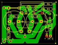
neutron7 said:another one
if anyone wants the files let me know
It's fine the way it is as far as GND configuration is concirned. If you can increase the size of the -/+V traces should be much better, BUT you can achieve similar result by just spreding a thick layer of solder on them, that will make them effectively thicker=wider. You can even run a piece of cupper wire soldered along the lenght of the +/-V traces. That'll be even better.
Changed it again, taking advice:
"move 0.1 closer to chip" (theChris)
"put ground around the edge" (Peter)
"make power traces thicker" (everyone!)
I am leaving the 1000u caps on the back of the board, because The dimensions fit better for my case that way than having a larger board.
Also i was thinking of having the copper side up anyways so it will be easy to remove the big caps if i need to. (havent decided yet)
I can always do it both ways and see which is better for me, simple flip horisontal in photoshop
Smoothed the edged of the traces, cant have those pesky electrons bouncing off corners and causing bad sound
Attachments
- Status
- This old topic is closed. If you want to reopen this topic, contact a moderator using the "Report Post" button.
- Home
- Amplifiers
- Chip Amps
- Please critique my Gainclone PCB