Update:
First off, let me say that I do not intend to cause a shouting match between the PCB lovers and the Point-to-Point (P2P) enthusiasts. I just noticed something interesting while prototyping so I decided to investigate and document it...
The story is this: I'm designing an amp based on the LM3886. My intent is to improve dramatically on the performance of the original LM3886. The final amp will reside on a PCB, but I figured I would build a prototype first. That way I could get the bugs ironed out before committing big bucks to a PCB fab run. I built the prototype using P2P wiring as that's the quickest and I expected it to provide as good performance as a PCB. Indeed the performance at 1 kHz was reasonably close to the data sheet figures.
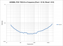
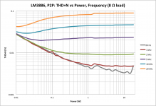
However, I was rather surprised when I measured the THD versus frequency. At 20 kHz the THD was an order of magnitude worse than the data sheet would indicate. This was rather surprising to me as the P2P circuit is pretty tight. The feedback network is right on the IC pins. As is the decoupling caps. The distance from the 1000 uF supply caps to the IC is not more than 40~50 mm. The circuit was fed from a quality lab supply.
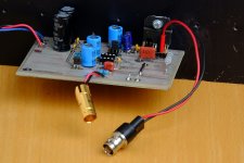
I decided to spin a quick prototype PCB. On the PCB is the exact same circuit as I used for the P2P setup. All the components came from the same batches of parts. Yet, on the PCB, I am able to reproduce the data sheet performance. The THD is much improved. The ground plane on the PCB is connected to the power ground. Signal ground runs as a separate trace and joins the power ground at the center between the two 1000 uF supply caps.
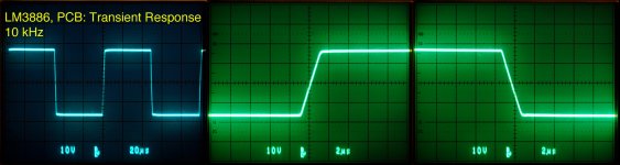
As seen from the transient responses, neither circuit exhibits tendencies towards instability. The transient response is nice and well controlled for both the PCB and the P2P circuit.
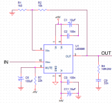
The schematic attached shows the main parts of the circuit. In addition, there are two 1000 uF electrolytic caps bypassed by two 47 nF ceramic caps where the power enters the board.
I suspect the return paths for the various electric fields in the circuit are better controlled in the PCB-based circuit. I am guessing that is the explanation for the difference.
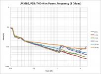
The abrupt change in THD around 1.5 W is caused by range switching in the HP 8903A distortion analyzer. The uptick in THD above 6 W for the 20 Hz trace is caused by brownout of the power supply.
The supply voltage was +/-28 V.
Equipment: HP 8903A distortion analyzer. Tektronix 2465B 400 MHz oscilloscope (using 20 MHz bandwidth setting to avoid interference from a nearby FM transmitter). HP 6228B power supply.
Just thought I'd share...
~Tom
- More comprehensive measurements available here: Post #30
- THD+N vs Frequency for inverting vs non-inverting configuration can be found here: Post #36
- THD+N vs Output Power for inverting vs non-inverting configuration can be found here: Post #38
- THD+N with star grounding is available here: Post #40
First off, let me say that I do not intend to cause a shouting match between the PCB lovers and the Point-to-Point (P2P) enthusiasts. I just noticed something interesting while prototyping so I decided to investigate and document it...
The story is this: I'm designing an amp based on the LM3886. My intent is to improve dramatically on the performance of the original LM3886. The final amp will reside on a PCB, but I figured I would build a prototype first. That way I could get the bugs ironed out before committing big bucks to a PCB fab run. I built the prototype using P2P wiring as that's the quickest and I expected it to provide as good performance as a PCB. Indeed the performance at 1 kHz was reasonably close to the data sheet figures.
However, I was rather surprised when I measured the THD versus frequency. At 20 kHz the THD was an order of magnitude worse than the data sheet would indicate. This was rather surprising to me as the P2P circuit is pretty tight. The feedback network is right on the IC pins. As is the decoupling caps. The distance from the 1000 uF supply caps to the IC is not more than 40~50 mm. The circuit was fed from a quality lab supply.
I decided to spin a quick prototype PCB. On the PCB is the exact same circuit as I used for the P2P setup. All the components came from the same batches of parts. Yet, on the PCB, I am able to reproduce the data sheet performance. The THD is much improved. The ground plane on the PCB is connected to the power ground. Signal ground runs as a separate trace and joins the power ground at the center between the two 1000 uF supply caps.
As seen from the transient responses, neither circuit exhibits tendencies towards instability. The transient response is nice and well controlled for both the PCB and the P2P circuit.
The schematic attached shows the main parts of the circuit. In addition, there are two 1000 uF electrolytic caps bypassed by two 47 nF ceramic caps where the power enters the board.
I suspect the return paths for the various electric fields in the circuit are better controlled in the PCB-based circuit. I am guessing that is the explanation for the difference.
The abrupt change in THD around 1.5 W is caused by range switching in the HP 8903A distortion analyzer. The uptick in THD above 6 W for the 20 Hz trace is caused by brownout of the power supply.
The supply voltage was +/-28 V.
Equipment: HP 8903A distortion analyzer. Tektronix 2465B 400 MHz oscilloscope (using 20 MHz bandwidth setting to avoid interference from a nearby FM transmitter). HP 6228B power supply.
Just thought I'd share...
~Tom
Attachments
-
 LM3886_Schematic.png17.3 KB · Views: 8,225
 -
 LM3886_PCB_Transient10kHz.jpg271.1 KB · Views: 7,971
 -
 LM3886_PCB_THD_vs_Freq_15W.png80.2 KB · Views: 7,607
 -
 LM3886_PCB_THD_PowerFreq.png135.6 KB · Views: 7,367
 -
 LM3886_P2P_Detail.jpg425.5 KB · Views: 3,398
 -
 LM3886_P2P_Full.jpg419.5 KB · Views: 3,785
 -
 LM3886_PCB.jpg348.7 KB · Views: 3,811
 -
 LM3886_P2P_THD_vs_PowerFreq_15R22nF.png119.9 KB · Views: 2,113
 -
 LM3886_P2P_THD_vs_Freq_15W.png82.8 KB · Views: 1,872
 -
 LM3886_P2P_15R22nF.jpg241.5 KB · Views: 7,293
Last edited:
I think we may have crossed edits... I realized I uploaded the wrong file for one of the pictures so I went back and changed it.
Nope. Not a Myref. Something better...
~Tom
That's intriguing, what is it then?

About those big bucks... you know you can get 10 of 50x50mm PCBs for about $10-$12, right? Probably even cheaper with a bit of googling, but this is a vendor I've used before.
Interesting facts ,we need more pictures and the better design schematic over the My_ref
That we do need.
Have you used the black speaker terminal as your Main Audio Ground?
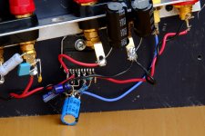
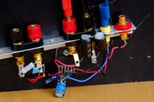
There are two black terminals. The one with the banana test lead plugged in is the power ground. This goes to the ground star (where all the passives come together). From the ground star runs a wire to the other black terminal (speaker negative) and to the shield of the input RCA connector.
During the test, the differential input on the HP8903A was used. I.e. its ground was lifted. This eliminated the possibility of a ground loop (and did improve the THD measurements).
Are the two sets of decoupling capacitors and the Output Zobel connected to the Power Ground?
The output Zobel is on the speaker terminals. That should be pretty obvious in the picture. I changed the Zobel to 22 nF polypropylene and 15 Ω (just as I have on the PCB) before I took the measurements as the 2.0 Ω + 150 nF shown in the picture caused stability issues.
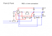
Does every circuit follow strictly the two wire close coupled pairs technique?
In the P2P setup, the input connection and output connections are twisted pairs. They're short, so they don't have many twists in them. But they are as closely coupled as I could make them. On the PCB, I run the traces pseudo-differentially. I.e. signal forward and return are tightly coupled.
Can you post PCB layout?
The relevant bits attached. I've grayed out the op-amp area (both for clarity and to avoid further confusion/speculation). Keep in mind that this is a prototype circuit slapped together quickly. There are some obvious optimizations to be made on the PCB. I'll leave those as an exercise for the reader...
BTW, I did not use the L||R Zobel network that you see in the PCB. R3 was a wire link (black wire on the board in the picture). Same is true in the P2P circuit.
That we do need.
I think so anyway... I'm afraid I've led the discussion astray by indicating that I'm working on something cool. Sorry about that. I would like to refocus this thread on LM3886 P2P vs PCB rather than letting it spin into a rumor mill. Once I'm ready with my circuit, I'll post a new thread and get a page started on my website. That's probably a month or two out. (Those are Engineering Months, so figure 3-4 calendar months...
)~Tom
Attachments
Last edited:
that is not what I think I can see.There are two black terminals. The one with the banana test lead plugged in is the power ground. This goes to the ground star (where all the passives come together). From the ground star runs a wire to the other black terminal (speaker negative) and to the shield of the input RCA connector.
During the test, the differential input on the HP8903A was used. I.e. its ground was lifted. This eliminated the possibility of a ground loop (and did improve the THD measurements).
The output Zobel is on the speaker terminals. That should be pretty obvious in the picture. I changed the Zobel to 22 nF polypropylene and 15 Ω (just as I have on the PCB) before I took the measurements as the 2.0 Ω + 150 nF shown in the picture caused stability issues.
In the P2P setup, the input connection and output connections are twisted pairs. They're short, so they don't have many twists in them. But they are as closely coupled as I could make them. On the PCB, I run the traces pseudo-differentially. I.e. signal forward and return are tightly coupled.
................
Take the input pair.
The red with is presumably signal.
The black wire must then be signal return.
It starts off as a twisted pair.
The black drops off and is connected to the black capacitors. WHY?
The red wire continues alone. It has lost it's close coupled partner.
The components on the left pair of terminals cannot be the Output Zobel. They are not mounted on the Output pin and the HF decoupled Power Ground.
I could go on.
I asked the questions to prompt you into looking again at your P2P assembly.
To me, it just does not follow any good practice.
Mark states:
IMHO your P2P is not the best it could be.
Last edited:
that is not what I think I can see.
Take the input pair.
The red with is presumably signal.
The black wire must then be signal return.
It starts off as a twisted pair.
The black drops off and is connected to the black capacitors. WHY?
The red wire continues alone. It has lost it's close coupled partner.
If you outline your understanding of the science behind why the performance should be better with the input ground (black wire) connected to the star ground by the other passives rather than the star by the supply caps, I'll be happy to move it and retake the measurements.
The components on the left pair of terminals cannot be the Output Zobel. They are not mounted on the Output pin and the HF decoupled Power Ground.
The gray resistor and the two caps in parallel (100 nF, 47 nF) are the output Zobel. That circuit was changed to 15 ohm, 22 nF as the 2 ohm, 150 nF caused stability issues.
I asked the questions to prompt you into looking again at your P2P assembly.
I'm completely OK with that. I would, however, prefer that you be specific and, preferably, outline the reason for your suggested changes. Referring to some arbitrary "best practices" doesn't carry much weight, honestly.
To me, it just does not follow any good practice.
To me, the circuits are functionally identical. Neither circuit shows issues with stability or ground loops. If you know of any scientific explanation of why changing the grounding will improve the HF THD, I'm all ears. Right now what I'm hearing is "this doesn't follow "best practices" (whatever that might be)" without any explanation of how you would prefer the layout to be and why your "best practices" will improve the performance of the circuit.
I'm all about discussing the circuit and the layout. But please back you claims up with a logical explanation based in science so we can keep the debate scientific rather than emotional.
~Tom
Last edited:
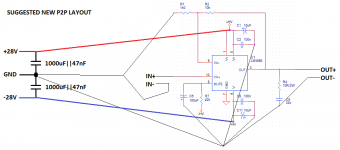
How about this? The new P2P "layout" will be exactly what I have on the PCB (that provides the performance specified in the datasheet, may I add).
If you have any suggestions for changes, please get them in so I can minimize the amount of changes. I plan to get the measurements done tonight (US Pacific time, GMT-8).
~Tom
If you have any suggestions for changes, please get them in so I can minimize the amount of changes. I plan to get the measurements done tonight (US Pacific time, GMT-8).
~Tom
Attachments
Mark, check your scheme. The amp won't behave properly.
regards
Sorry, I don't see it.
the + input needs a dc path to somewhere. A 47k resistor from the 1k-2uF junction to ground would be just fine.
Same for Toms wiring plan. If his amp ever gets disconnected from a dc-coupled source the output could set itself to an undefined dc-level and fry an attached speaker.
Same for Toms wiring plan. If his amp ever gets disconnected from a dc-coupled source the output could set itself to an undefined dc-level and fry an attached speaker.
Last edited:
the + input needs a dc path to somewhere. A 47k resistor from the 1k-2uF junction to ground would be just fine.
Yes, I see what you mean, Tomchr has no pot at all and no resistor between input and ground. It's more to demonstrate how not to mix signal returns and which leads need to be kept short.
- Home
- Amplifiers
- Chip Amps
- LM3886 PCB vs Point-to-Point (with data)