Hi all,
Just ordered LM3886 kit from Analogmetric :
2x LM3886 68W Power Amplifier Kit (Mono)_Solid-State Amp_Analog Metric - DIY Audio Kit
I have not found the schematic, but I think it's the same like this one :
http://audio.claub.net/other_stuff/LM3886 XY power amp pcb schematic with components labeled.jpg
from this thread :
http://www.diyaudio.com/forums/chip-amps/196123-lm3886-pcb-3.html
Right ?
Thank's.
Phil.
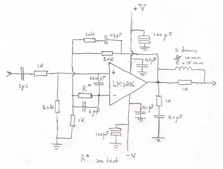
Yep, I got almost the same kit, and this is the right schematic. You should consider adding a 220pF capacitor between pin 9 and 10 on the LM3886. I've read that this should filter out potential RF noise or something. You can also find this in the datasheet for the IC.
I soldered a poly cap directly to the pins, under the PCB. If you want to read more about improvements to this particular PCB design, read THIS POST!
I soldered a poly cap directly to the pins, under the PCB. If you want to read more about improvements to this particular PCB design, read THIS POST!
Thank's !!
So schematic was :
May I can fix input impedance by changing R5 ?
Phil.
So schematic was :
An externally hosted image should be here but it was not working when we last tested it.
May I can fix input impedance by changing R5 ?
Phil.
Don't put C6 between pin 9 and 10 but instead put C6 across R5. If you are not convinced, look at the pictures on your scoop with a block signal at the input and you will see the difference.
Can I ask you Marc Vi, what does the scope show? I'm on vacation right now, so I can't test this for another month.
Thanks a lot! I saw a post about putting a 220pF cap across R5, but every schematic showed that it was connected through pin 9 and 10!
The kit we both own doesn't have a zobel network and an inductor at the output. Is this really necessary? Of course I'll add it if it's necessary 🙂
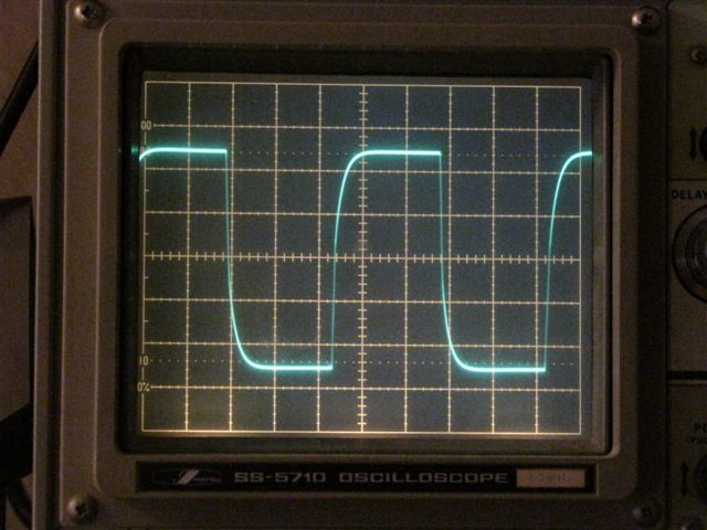
So this is the picture of a 20kHz square wave with a 220pF across R5, right?
The kit we both own doesn't have a zobel network and an inductor at the output. Is this really necessary? Of course I'll add it if it's necessary 🙂
So this is the picture of a 20kHz square wave with a 220pF across R5, right?
Last edited:
Yes, this is the picture of a C accross R5.
I believe what every schematic shows untill I see something else and then I believe my own eyes.
I do have a Zobel network and an inductor at the output. The inductor does only influence the output when you make the output capacitive, say with 2 microFarad. Then you see ringing and that is normal and it prevents the amplifier from oscillating.
They say that you need a Zobel network for a complex loudspeaker. I have never seen the difference - maybe because my speaker is not so complex - but it doesn't harm either.
Marc.
these are my current loudspeakers. I won't call them complex, but they have a crossover inside. SEAS Mimir
I'm not worried about adding a zobel at the output. Thats seems like an easy job. The problem is in the input side. Your schematic (in the post you posted) looks a bit different than mine, and I don't think there is possible to make the same circuit as you have.
the 20k resistor and 47pF capacitor seems to crash with R3 in the schematic in the third post 🙁 I also don't have the R* resistor in your schematic.
Please don't interchange my schematic with yours because it has other purposes! Therefore you must read my thread more thoroughly.
The only thing you have to do is to take your schematic and place the C of 220 pF between pin 9 and pin 10 and then put it over R5 and see the difference.
Marc.
The only thing you have to do is to take your schematic and place the C of 220 pF between pin 9 and pin 10 and then put it over R5 and see the difference.
Marc.
Hi all,
What do think of placing C 220 pF directly at the input, like this :
I think Rin is the imput impedance, right ?
I need to fix this value to calculate a passive line level xover..
Thank's.
Phil.
What do think of placing C 220 pF directly at the input, like this :
An externally hosted image should be here but it was not working when we last tested it.
I think Rin is the imput impedance, right ?
I need to fix this value to calculate a passive line level xover..
Thank's.
Phil.
The RF attenuation is the same.
But the impedance seen by the +IN pin is set mainly by R5 and R6+C5 in parallel.
If C6 is installed parallel to R5 then +IN sees R5||[R6+C5||C6.
This lowers the HF impedance significantly.
Most BJT inputs benefit from a low source impedance.
The Reason for removing C6 from the -IN pin is that capacitance on the -IN pin can promote instability. R4 should be mounted very close to -IN pin.
Thank's Andrew..
So, what's your best advice for RF attenuation ?
If I change C5 (1 uF) by 3.3 uF, how calculate the new input impedance ?
Below the pcb from Analogmetric with explained componants :
I think R4 is very close to -IN pin..
I don't know were is C1 C2 and C3, so I have appointed A B and C..
Phil.
So, what's your best advice for RF attenuation ?
If I change C5 (1 uF) by 3.3 uF, how calculate the new input impedance ?
Below the pcb from Analogmetric with explained componants :
An externally hosted image should be here but it was not working when we last tested it.
I think R4 is very close to -IN pin..
I don't know were is C1 C2 and C3, so I have appointed A B and C..
Phil.
The RF attenuation parallel to R5 as posted by Marc and myself !!!!
Reverse engineer the PCB
And find where the Power Ground (between the +ve and -ve Power Input terminals)
meets the Signal Ground (to the left of the Signal Hot terminal).
Find also what other components share the trace between Power Ground and Signal Ground. Particularly WHERE they tap in. Draw out a MAP of the GROUND trace with all the tapping points.
The designer almost certainly will have this WRONG !
Thank you again Andrew, I appreciate your help !
And sorry for my basic questions..
I found a thread about power ground, as you say (I think) :
http://www.diyaudio.com/forums/chip-amps/207971-bought-xy-lm3886-kit-40.html
and it show this "upgrade" :

Phil.
And sorry for my basic questions..
I found a thread about power ground, as you say (I think) :
http://www.diyaudio.com/forums/chip-amps/207971-bought-xy-lm3886-kit-40.html
and it show this "upgrade" :
Phil.
I had not seen this modification.
It looks like someone has reverse engineered that XY PCB and shown how to bypass the errors.
It looks like someone has reverse engineered that XY PCB and shown how to bypass the errors.
Not until someone reverse engineers that particular PCB and determines that it is correct.
You need to do that with YOUR PCB.
You need to do that with YOUR PCB.
Hi,
I just received the kit from AM..
To compare with LM3886 XY :

Not exactly the same !
I just received the kit from AM..
An externally hosted image should be here but it was not working when we last tested it.
To compare with LM3886 XY :
Not exactly the same !
- Status
- Not open for further replies.
- Home
- Amplifiers
- Chip Amps
- LM3886 kit from AM