Hi. I've been thinking a little bit and I started wondering about how crossover distortion and slew rate are connected. The design I'm thinking of is a single op-amp with an unbiased class B push-pull output stage. My thinking is that if the slew rate of the op-amp is high enough, the crossover distortion won't be audible as the output of the op-amp will be able to reach +0.6V to -0.6V quick enough not to have much of an impact on the output of the amplifier. Although my knowledge is limited in this area, I'm actually thinking that the crossover distortion can be directly calculated when knowing the slew-rate, output voltage level and output frequency, is this the case?
I did some simulation on circuitlab. While decreasing the slew rate does indeed increase crossover distortion, increasing the slew rate only decreases crossover distortion to a certain point, I expected to get zero visible distortion with an insane slew rate of 1GV/s, but this is not the case. Is this a flaw in the simulator, or are there other factors that I don't know about? While the slew rate I set for the op-amp could easily be calculated when feeding the amp with a square wave, I could not do the same when feeding it a sine wave. Take a look at this simulation: https://www.circuitlab.com/circuit/ynfes6/slew-rate-test/
The output of the output stage stops at 0V as expected, but I also expected the op-amp output to get from 0.6V to -0.6V as quickly as possible, but it doesn't. I thought the op-amp would make this jump in a linear fashion, but the result from the simulation show otherwise.
The reason I've been wondering about this is because I'm kind of intrigued by an unbiased class B push-pull stage. It's so simple, efficient and can potentially have a very high current output. A quick look at the op-amps available I find some with an insanely high slew rate, several hundred and even a thousand V/us. Is it possible to make an amplifier with close to inaudible crossover distortion using one of those op-amps?
Unbiased output stage is hard to make really clean. you have to transition a (round numbers) 1 volt deadband. Probably more if you use darlingtons to make the output stage easier to drive.
Even if the amp slews at 1000 V/us, it still takes 1 nanosecond to get through the dead-band. That however, isn't the long pole. The transistors take much longer than that to turn on. That will make for a bigger dead-band and notch.
If you're looking for a zero-biased output stage that can work pretty well, check out the old Peter Walker articles on current dumping.
Akitika GT-101 Audio Power Amplifier Kit
Update My Dynaco
Thanks for the reply. I scrolled through the links you gave me, but I'm not sure what I'm supposed to be looking for? There's no schematics or much technical info as far as I could see 
I've never really learned about the turn-on time of bjt's, I assume this has to do with some base capacitance? Is this possible to calculate? My firs thought was to make a very small amplifier so there would be no need for darlington pairs, it would also suffice with small transistor packages which are perhaps faster?
I've never really learned about the turn-on time of bjt's, I assume this has to do with some base capacitance? Is this possible to calculate? My firs thought was to make a very small amplifier so there would be no need for darlington pairs, it would also suffice with small transistor packages which are perhaps faster?
because I'm kind of intrigued by an unbiased class B push-pull stage. It's
so simple, efficient and can potentially have a very high current output.
Hi,
Biasing or not does not affect current output. CFP's have
a lower standing current than EFP's, but the efficiency at
higher powers is very near the same as the unbiased case.
CFP's also have lower biasing voltage than EFP's.
There is some argument for higher standing current to
reduce the temperature variations, but it will idle hotter.
Causing a problem, x/o distortion, and then trying to fix it
is never going to be as good as not causing the problem.
rgds, sreten.
rgds, sreten.
Plecto, I must agree with a previous poster, who said,
"Causing a problem, x/o distortion, and then trying to fix it
is never going to be as good as not causing the problem."
My apologies about the confusion I generated in posting those links, they are just part of my normal sign-off signature.
The analysis you want to do for transistor turn on time is best done using a technique called "charge control" analysis.
A work around that many have used for the configuration that you propose is to place a low-ish resistor from base to emitter of the transistors. That way, when the transistors are off, there is still some output from the opamp that makes it through to the speakers. Thus, in the previous 1 volt dead-band, the gain isn't zero, but rather given by a voltage divider between the added resistance and the load resistance.
Here's an example. If that resistance were 8 ohms, then the gain in the "dead band" region would be 1/2 (assuming an 8 ohm speaker), which while less than the limiting 1 of an active emitter follower, is a whole lot better than zero... It does say that the opamp would have to be able to deliver 0.6/8= 75 mA at the edge of the dead band, and a bit more than that once you need base current.
That may be more current than you could count on from a lot of op amps, but you get the general idea. Add it to your sims, and see its effect.
All the best...
Dan
Akitika GT-101 Audio Power Amplifier Kit
Update My Dynaco
Great idea djoffe, I did a simulation and it looked good, going to take another look later.
Yeah, I know that class AB has the same current output and potentially the same efficiency, but the simplicity of an unbiased output stage is still appealing to me. Mind that I'm not planning on making some hifi amplifier, all I want is to make the crossover distortion barely audible. I made an amplifier like this a while back with a NE5532 and MJE3055/MJE2955 BJT as an output stage. I'm pretty sure there are faster components I could use, but despite this, the amplifier was by no means unusable. The crossover distortion was only audible during higher frequencies, and I'm sure a lot of people wouldn't mind it. So again, how audible will the crossover distortion be if I choose to make it from very fast components?
Yeah, I know that class AB has the same current output and potentially the same efficiency, but the simplicity of an unbiased output stage is still appealing to me. Mind that I'm not planning on making some hifi amplifier, all I want is to make the crossover distortion barely audible. I made an amplifier like this a while back with a NE5532 and MJE3055/MJE2955 BJT as an output stage. I'm pretty sure there are faster components I could use, but despite this, the amplifier was by no means unusable. The crossover distortion was only audible during higher frequencies, and I'm sure a lot of people wouldn't mind it. So again, how audible will the crossover distortion be if I choose to make it from very fast components?
I never "got" the current dumping idea tbh because it relies on a (relatively) high dissipation Class A section to work and as such can be bettered dissipation wise by a properly designed Class (A)B stage. Its only advantage that I could see was no bias adjustment was needed in production.
As you figured out, you have a tradeoff between idle current and speed. It is cheaper to build an output stage with slow transistors and then use bias to reduce the size of the deadband, than it is to build an extremely fast output stage that can zip through a large deadband in a negligible time.
It is the speed of the output stage itself that matters, not the speed of the voltage amplifier driving it. If the output stage is slow, then you have to apply more compensation to the voltage amp to avoid instability of the feedback loop, and that makes it slower to respond to errors, thus worse at correcting the gain dip due to a lack of bias.
Even the Quad 405 applied some bias to its "dumper" transistors. It also skewed them off-centre so the crossover point didn't occur at exactly zero volts, and small signals could avoid it completely.
Last edited:
Short answer: Turn-on is pretty quick, but if the BJT has been conducting hard it could take up to a microsecond or two to turn off.
Long answer: Read the data sheet for the BJT you plan to use along with Bob Cordell's new book.
Even longer answer: Start by studying audibility of crossover distortion.
Long answer: Read the data sheet for the BJT you plan to use along with Bob Cordell's new book.
Even longer answer: Start by studying audibility of crossover distortion.
How do I calculate the turn on/off time of bjts? Even though I clearly see that biasing the output stage is no big deal, I would still like to understand the limitations of an unbiased output stage as well as perhaps make a design and do some measurements on it.
If you made a simple two transistor output stage and fed it with a pure sine wave you would see how little bias is needed for the distortion to audibly disappear. Its very instructive. Do you have a "real" scope ?
If you made a simple two transistor output stage and fed it with a pure sine wave you would see how little bias is needed for the distortion to audibly disappear. Its very instructive. Do you have a "real" scope ?
I have a real scope yes. I know that it's possible to bias the stage to the point where it 'almost' conducts to avoid just about all crossover distortion. I've biased a class AB output stage in the past using two diodes between the bases, but this solution will either lead to a high bias current or low output voltage swing. I'm thinking that a solution would be to have four resistors setting the bias point, that won't limit the output swing that much, but it will still limit it. An unbiased output stage doesn't have these issues.
Back to the speed of a bjt though. Isn't there some theory that can be calculated? Calculate some RC time constant for a bjt modeled with some resistors, caps and a current source or something (think I remember doing something like that at uni)?
Bias current doesn't affect voltage swing as you seem to suggest, something is wrong if you find it does. To accurately set bias and to set it such that its maintained over a wide range of conditions (supply, temperature) needs nothing more than a vbe multiplier. Fixed bias with diodes and so on tends to be hit and miss.
Bjt switching speed and turn off effects are easily and practically demonstrated with a scope. How wouldn't have a clue how to calculate it as it depends on how quickly charge carriers can be pulled from the base region of the device... thats getting into physics.
Bjt switching speed and turn off effects are easily and practically demonstrated with a scope. How wouldn't have a clue how to calculate it as it depends on how quickly charge carriers can be pulled from the base region of the device... thats getting into physics.
Back to the speed of a bjt though. Isn't there some theory that can be calculated? Calculate some RC time constant for a bjt modeled with some resistors, caps and a current source or something (think I remember doing something like that at uni)?
The resistor-cap-current source thing is called the hybrid-pi model. The Cordell book contains worked examples showing how to calculate turn-off times with it.
File:Hybrid-pi detailed model.svg - Wikipedia, the free encyclopedia
The effective input capacitance in the model turns out to be several microfarads, and the usual designs of driver stages only have limited current available to discharge it.
hybri-pi is a small signal linear model doesn't show the larger turn on/off effects which are nonlinear - all of the terms in the linear model change by large factors over turn on/off conditions
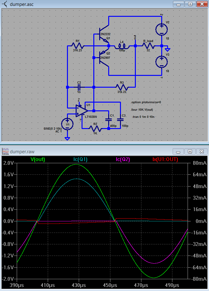
I did sim a "Current Dumping" circuit which could be vieiwed as a smarter way to add the op amp fast slew to the unbiased output Q http://www.diyaudio.com/forums/soli...r-requirements-class-c-ab2-2.html#post2388517
and many here use the free, unlimited LTspice - not as newbie friendly - but very powerful if you already know Spice
Last edited:
- Status
- This old topic is closed. If you want to reopen this topic, contact a moderator using the "Report Post" button.
- Home
- Amplifiers
- Chip Amps
- Crossover distortion and op-amp slew rate