I'm using a 220r input resistor (Rb) on an LM3886 amp and currently have it wired BEFORE Rin instead of after it like it is on the datasheet. I've already etched the pcb/soldered all the parts in and the amp sounds fine, maybe a little quiet, but otherwise fine. The DC offset is fine.
Am I screwing anything up wiring that way? I can probably re-wire using jumpers and scratching out traces if need be to fix the problem.
Am I screwing anything up wiring that way? I can probably re-wire using jumpers and scratching out traces if need be to fix the problem.
Sounds from your description that the layout will be OK.
The series resistor needs to be before the RF attenuating capacoitor.
Similarly the Series capacitor needs to be before the DC attenuating resistor going to signal ground.
The order of these two pair of components can be moved around. Just keep the individuals of the pairs in the correct order.
The series resistor needs to be before the RF attenuating capacoitor.
Similarly the Series capacitor needs to be before the DC attenuating resistor going to signal ground.
The order of these two pair of components can be moved around. Just keep the individuals of the pairs in the correct order.
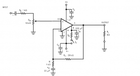
why are you still using that stripped down schematic?A very quick edit to show what I did (except Rb is 220r):

why are you still using that stripped down schematic?
Laziness and complacency since it worked when I tried it and had already made the PCBs, largely

In all reality, though, the PCB layout as designed could pretty easily accommodate a Zobel retrofitted. I just kind of wanted to make sure I wasn't screwing up the essentials like when I wired the gain resistors wrong on accident and ended up with 27 volts of DC offset. Had to say goodbye to that $1.99 RCA 20 watt speaker I found at a closeout place that day!
On a (semi) related note: if I am using a potentiometer on the input, would it make sense to delete the input resistor?
That is another component you would be omitting.if I am using a potentiometer on the input, would it make sense to delete the input resistor?
Place a DC blocking capacitor on the input.
That DC blocking capacitor isolates the input from the variable resistance of the pot.
Variable resistance affects the input bias !
That is another component you would be omitting.
Place a DC blocking capacitor on the input.
That DC blocking capacitor isolates the input from the variable resistance of the pot.
Variable resistance affects the input bias !
Isn't that what I have there? I have a tiny electrolytic capacitor in series before the resistor. Or do I need another one?
A very quick edit to show what I did (except Rb is 220r):
I wish you would attach your schematic.
You don't know how much work it is for me to bypass my computer virus protection to view a file stored in a site that has known virus issues.
I'm sorry to say this to someone who has had pcbs made, but of all the ways to use a 3886, this one must be among the worst. There is so much wrong with it.
What might rescue it a little is a capacitor to ground on the input, in parallel with your pot or Rin. You want somewhere around 100kHz. And a resistor between that an Vin+, of around 50R. (Go and see Siegfried Linkwitz's page of 3886s).
What might rescue it a little is a capacitor to ground on the input, in parallel with your pot or Rin. You want somewhere around 100kHz. And a resistor between that an Vin+, of around 50R. (Go and see Siegfried Linkwitz's page of 3886s).
I wish you would attach your schematic.
You don't know how much work it is for me to bypass my computer virus protection to view a file stored in a site that has known virus issues.
Sorry! Imgur is widely used on the internet and I assumed it would be fine!
I'm hearing a consensus "make a new one using a different schematic that isn't nearly as terrible for a beginner" which I am totally willing to do in the interest of having the best amp possible (I mean, they're like 2 dollars to build it on a new pcb if I scavenge the expensive stuff), but I'm still very interested in knowing for my own understanding:
1) Does moving the input resistor like I did cause problems?
2) Is the input resistor made redundant by a pot?
Attachments
The input bias current to the -IN is fed in via Rf1 (20k) from the low impedance of the Output Pin and the 8ohms speaker load.
The input bias current to the +IN pin is fed in via the variable volume potentiometer. That can vary from 0k0 to 10k0.
This WILL CHANGE the output offset. BAD !!!!
This will also make the output offset CHANGE more with changes in chip temperature. BAD !!!!
You must fit an resistor to set the input bias current to match the -IN pin's bias.
Then you should fit a DC blocking capacitor to prevent the vol pot from changing that bias current.
This achieves TWO desirable outcomes.
a.) you can set the output offset to very close to 0mVdc at either cold, or warm, or hot.
b.) the balanced input bias currents make the temperature sensitivity of the output offset much smaller. The output offset stays nearly constant over a sensible range of operating temperatures.
Next.
The output of the amplifier sees 20k as a load and it also sees the reactance of the speaker and it's cabling and the reactance of the wire connecting PIN3 to the speaker terminal.
The amplifier if fed with HF interference needs to see an HF load to allow it to work properly.
This HF load is the output Zobel.
FIT IT !!!!
Check Ci.
You should NOT have any significant voltage across it.
Interference:
Add an RF interference filter to the input of the amplifier.
Consider also adding and interference filter after the Output Zobel.
After re-reading that about 20 times and reading way more about input bias current than I thought I'd ever do on a Friday afternoon, let me try to unpack what you just said
When looking just at what's going into pin #10, an input signal should:
1. Leave the source
2. Enter a 10k pot which could vary by 0k-10k
3. Leave the pot into a capacitor in series to block DC
4. Leave the DC blocking capacitor and see 2 paths: a 10k resistor to ground and a 1k resistor leading to pin #10.
The 1k resistor is then the part we are focusing on for your first part, right? 1k is I'm assuming specifically chosen to balance the positive input bias current with the 8 ohm speaker+20k resistor on the negative side? A 4 ohm speaker would therefore require a different value if I'm interpreting you right as well.
Zobel: Easy enough. Looking around at designs it would appear that the values chosen for the resistor and capacitance vary widely. Any thoughts on values? Do these change the values for the input bias current?
RF interference filter: Is this made the same way as the output filter? I didn't find too many examples of people using an inductor/resistor combination on the input.
Also: AndrewT, you're awesome! I mean, I sometimes have to watch an EEVblog video or 2 and read a couple wikis to even come close to grasping what you just said, but that's what I get for getting an MBA instead of an MSEE
It's a non-issue in the real world, as long as your DC gain is unity. Mismatched bias resistance path will add 1mV per kOhm additional worst case current offset on top of the 10mV worst case voltage offset, with a 20k mismatch that's 30mV worst case instead of 10mV (and typically 1/10th of it).The input bias current to the -IN is fed in via Rf1 (20k) from the low impedance of the Output Pin and the 8ohms speaker load.
The input bias current to the +IN pin is fed in via the variable volume potentiometer. That can vary from 0k0 to 10k0.
This WILL CHANGE the output offset. BAD !!!!
This will also make the output offset CHANGE more with changes in chip temperature. BAD !!!!
Of course one should never rely on a pot wiper alone to bias a pin, it may lift and then the output will go to a rail, so something like a 20k...100k "fallback" resistor is a good idea.
the +IN pin sees the 1k and 10k in series = 11k.Leave the DC blocking capacitor and see 2 paths: a 10k resistor to ground and a 1k resistor leading to pin #10.
The 1k resistor is then the part we are focusing on for your first part, right?
That is 9k different from what the -IN pin sees (20k).
So you change the 10k shunt to ground resistor to 20k giving a total of 21k and measure the actual offset. Is it +ve or -ve offset? Add an parallel resistor of 100k across the new 20k. Is the offset +ve or _ve? is is smaller or larger than it was.
This tells you what to do to that 20k to minimise the output offset. That also minimises the change in offset with temperature.
- Status
- This old topic is closed. If you want to reopen this topic, contact a moderator using the "Report Post" button.
- Home
- Amplifiers
- Chip Amps
- LM3886 Input Resistor Position