Hi everyone and thanks in advance.
I've run into some real grief with my little chipamp, and since I'm from a valve background (and no longer have access to my old lab tools, like an o-scope), the symptoms are baffling me.
Here goes:
The circuit:
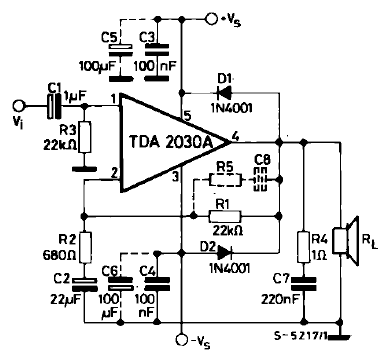
I'm using a TDA2030 in a noninverting circuit, as recommended by ST Micro's datasheet (and using the same values). My first wiring effort was botched by omitting part of the circuit - I wasn't that surprised that it failed. My second effort however, was "by the book" - everything was there except for the series resistor/cap that's parallelled to the feedback resistor (which is not on one of the schematics - I'll put it in my next one).
The construction:
It's all point to point (hey, I AM a valve guy after all....), with a 2" lead from the last decoupling caps in the power supply to the chip's V+/V- pins. The pins themselves were bent to accomodate the small parts like the feedback resistor and the protection diodes - I've got them actually fitted between the pins with essentially no lead length.
The power supply:
25VCT nominally, I measure 29VAC at it's secondary taps and about 37VDC after rectification and filtering. In theory the TDA2030A is rated to +/-18V and it's seeing about +/-18.5V at the supply pins.
The symptoms:
At first power on there is measurable AC on the load resistor (no way am I risking loudspeakers on THIS one yet). However, it soon departs, to be replaced by DC, which climbs to around 16VDC (protection diodes or not!). No overheating (or heating of any kind for that matter) is experienced. However, while testing various voltages on the chip late last night the most remarkable thing happend - with a flash of lightning and a loud *CRACK* about half the chipface disintegrated, exposing some of the metal pins! Good thing I was wearing glasses..... Fortunately the PS, input source (portable CD player) and such were not damaged. I'm a bit mystified as to what happened there, since I don't think I accidentally shorted anything at the chip. I did have the negative lead of my DMM on the star ground rather than at the chip - could that have been contributory or even causative?
The questions:
1. Is it overvoltage, oscillation (there's no overheating and there's no way I can hook it up to an o-scope to be sure), or something else?
2. Do my .1uF decoupling caps have to be attached right at the pins of the chip, or am I okay to leave 2" leads going from the PS board (i.e. should I add some more .1uF caps? Another trip to the electronics store coming up....)?
3. If it's overvoltage, what's the best way to drop my PS voltage down to say +/-16V? A voltage divider? A 7815 and a 7915? (don't have any on hand and packing 'em in that enclosure's not going to be easy - it's pretty crowded now....). How 'bout a simple series resistor? If all fails would a 2.5A diode to each pin be okay - my guess is that I'd DEFINITELY need a decoupling cap after a "dropper diode".
Sorry for being such a dunce, but this is turning out to be truly humbling. I know what to look for in a valve circuit that's gone west, but this newfangled IC stuff is something I usually don't work with.....except with low powered battery PS headphone amps (never had a stitch of grief there!).
Thanks in advance for your patience and help.
All the best,
Morse
I've run into some real grief with my little chipamp, and since I'm from a valve background (and no longer have access to my old lab tools, like an o-scope), the symptoms are baffling me.
Here goes:
The circuit:
I'm using a TDA2030 in a noninverting circuit, as recommended by ST Micro's datasheet (and using the same values). My first wiring effort was botched by omitting part of the circuit - I wasn't that surprised that it failed. My second effort however, was "by the book" - everything was there except for the series resistor/cap that's parallelled to the feedback resistor (which is not on one of the schematics - I'll put it in my next one).
The construction:
It's all point to point (hey, I AM a valve guy after all....), with a 2" lead from the last decoupling caps in the power supply to the chip's V+/V- pins. The pins themselves were bent to accomodate the small parts like the feedback resistor and the protection diodes - I've got them actually fitted between the pins with essentially no lead length.
The power supply:
25VCT nominally, I measure 29VAC at it's secondary taps and about 37VDC after rectification and filtering. In theory the TDA2030A is rated to +/-18V and it's seeing about +/-18.5V at the supply pins.
The symptoms:
At first power on there is measurable AC on the load resistor (no way am I risking loudspeakers on THIS one yet). However, it soon departs, to be replaced by DC, which climbs to around 16VDC (protection diodes or not!). No overheating (or heating of any kind for that matter) is experienced. However, while testing various voltages on the chip late last night the most remarkable thing happend - with a flash of lightning and a loud *CRACK* about half the chipface disintegrated, exposing some of the metal pins! Good thing I was wearing glasses..... Fortunately the PS, input source (portable CD player) and such were not damaged. I'm a bit mystified as to what happened there, since I don't think I accidentally shorted anything at the chip. I did have the negative lead of my DMM on the star ground rather than at the chip - could that have been contributory or even causative?
The questions:
1. Is it overvoltage, oscillation (there's no overheating and there's no way I can hook it up to an o-scope to be sure), or something else?
2. Do my .1uF decoupling caps have to be attached right at the pins of the chip, or am I okay to leave 2" leads going from the PS board (i.e. should I add some more .1uF caps? Another trip to the electronics store coming up....)?
3. If it's overvoltage, what's the best way to drop my PS voltage down to say +/-16V? A voltage divider? A 7815 and a 7915? (don't have any on hand and packing 'em in that enclosure's not going to be easy - it's pretty crowded now....). How 'bout a simple series resistor? If all fails would a 2.5A diode to each pin be okay - my guess is that I'd DEFINITELY need a decoupling cap after a "dropper diode".
Sorry for being such a dunce, but this is turning out to be truly humbling. I know what to look for in a valve circuit that's gone west, but this newfangled IC stuff is something I usually don't work with.....except with low powered battery PS headphone amps (never had a stitch of grief there!).
Thanks in advance for your patience and help.
All the best,
Morse
2. Do my .1uF decoupling caps have to be attached right at the pins of the chip, or am I okay to leave 2" leads going from the PS board (i.e. should I add some more .1uF caps? Another trip to the electronics store coming up....)?
Definitely near the chip IMO.
I suspect you haven't done this :
The power supply should have 2,200uF to 3,300uF per rail.
The 100uF capacitors should be mounted on the end of the PS leads.
The 0.1uF capacitors should be near the chipleads.
Suspect oscillation. Voltage appears to be well within specification.
Can't find a good explanation of R5 and C6 in the data sheet,
on the feedback resistor from the typical application.
Also the typical application has very poor grounding practice,
I hope you haven't followed it.
You should have separate ground returns for the input/feedback, power
supply decoupling and the return from the load to the star point.
") sreten.
sreten.Thanks Sreton;
Okay, so my +/-18.5Vs shouldn't toast a +/-18Vmax TDA2030, and oscillation is the prime suspect. I'm just about to head off to the electronics shop and stock up on .1uF 100V mylars (fresh out now...and my usual 600V film and foil caps are WAY too big).
Thanks for the tip on grounding. My original grounds scheme was a little better than what's shown, but I'd shared the input/feedback ground with the load return ground. Time to put in a longer return wire, straight to the star ground.
Also, I've got the 1ohm resistor/.22uF cap load protector wired directly to the speaker terminals - should this be a problem? My DMM shows a .1ohm increase in the resistor due to the 4" lead length....
>>>...Can't find a good explanation of R5 and C6 in the data sheet, on the feedback resistor from the typical application...<<<
The spec sheet is more than a little confusing on R5/C8; it claims the combo is there for high freq cutoff and that C8 should have a value of 1/(2*pi*R5*Br) and I presume tha t Br should be the high freq f3 - in my case 20,000 cps. It looks to me like the impedence of R5/C8 will decrease as the signal freq increases, thus high freq signals will have more feedback cancellation. Is that right?
One last question - any reason not to use 1/8 ohm resistors for things like the feedback resistor? They're far easier to work with when wiring directly to the pins than are the 1/4 watt resistors I'm using.
Thanks again and all the best,
Morse
Thanks Sreton;
>>>...F3 shoud be more like 50KHz...<<<
That helps!
>>>...The spec sheet...quotes output at 19-0-19V
and gives the maximum as 22-0-22V, so i'm not sure
were you've got the 18-0-18V maximum from...<<<
My spec sheet I'm quoting is dated 1993, so there must be an update out there that I don't have. I'll look 'round and see what I can find....
Thanks again!
All the best,
Morse
Hi OFB;
>>>...wouldn't oscillation heat up the chip?...<<<
That's what's been confusing me. However, Sreten is quite correct. I just checked the newest datasheet on the TDA2030A (which is what I have been using) and it shows Vabsolute max = +/-22VDC, leaving me with several volts of overhead. FWIW, there was a LOT of heat generated locally when the one TDA2030A came unglued. Never seen anything like it....
Thanks and all the best,
Morse
Hi everyone - this is really becoming a bothersome project, so any and all suggestions (that are printable and do not involve long walks off short piers and suchlike) are welcome!
Update:
As of now, the third incarnation of the circuit (just trying to get one channel to work right before building the second....) is better than the first two - but that's not saying much. I have 33mV of hum (!!!!!!), a heckuva turn-on and turn-off bounce, and no music - unless you want to count a kind of severe distortion that creeps up at extremely high volume levels. The "distortion" does indeed seem to be the music signal, albeit so severely distorted that it sounds more like blasts of static "in time" with the music.
Oscillation? If so, I've never heard it this bad in ANY circuit (including my first attempt at a 6DJ8 that rang like a bell and would go into oscillation at the drop of a hat - but that's another story...).
Damage to the chip? I'm not really an expert at hand soldering IC chips, and it's been a lamentable 4 months since I've logged serious quality time with my soldering station. However, I held onto the chip with thumb and forefinger while soldering - it became warm (even hot) but not too hot to hold. And from experience that says it's less than 60C. Could it have "locally" heated and damaged the innards of the device?
Something else?
Here are the changes to the 3rd gen circuit:
I used .1uF 50V ceramic discs from Radio Shack for the decoupling caps at the +/-Vs pins on the chip. Both caps connect together and the common lead is used for a ground line running directly back to HQ ground point.
The signal return lead now has a dedicated line to HQ ground that is separate from the input decoupling line - this connects to the ground line on the potentiometer and has a dedicated line back to HQ ground that's a good 6" to 7" long.
A 1500pF cap was used inline with a 2000 ohm 1/8 watt resistor as the R5/C8 cap series in the feedback loop. Both parts were directly measure for value to ensure that an inadvertant substitution had not occurred.
I did substitute 1N4007's for the 1N4001's in the original schemo, since I have plenty of the former and none of the latter on hand. Problem?
One thing that should be mentioned earlier is that I omitted R4 in the schemo, substituting a 100k ohm pot in advance of the 1uF coupling cap.
As it is now, I'm seriously considering the insertion of a pair of 2200uF caps in the output stream for decoupling, just to cut out that startup and shutdown surge.
Frankly I can't see ANYTHING wrong with this circuit or my implementation of it - no solder bridges, cruddy joins or such are evident, and the PS is performing flawlessly.
HELP!!!!
Thanks in advance and
All the best,
Morse
Thanks for posting the schemo, OFB;
Yep, that's the circuit. Most grief I've had debugging anything in mucho years! It's not made easier by being such a simple little critter.....
One other little change is that I'm using 2200uF instead of 100uF for the first stage decoupling caps (used what I had on hand), and there's an extra .1uF decoupling stage fitted at the PS caps that's going to be shared by both channels.
Also, there is an LED running from V+ to V-, biased to about 9mA.
>>>...geeze morse, you're just charmed...<<<
*LOL*! When things like this happen, I like to kid around that I'm obviously paying for some delightful villainy in a past life....
All the best,
Morse
Yep, that's the circuit. Most grief I've had debugging anything in mucho years! It's not made easier by being such a simple little critter.....
One other little change is that I'm using 2200uF instead of 100uF for the first stage decoupling caps (used what I had on hand), and there's an extra .1uF decoupling stage fitted at the PS caps that's going to be shared by both channels.
Also, there is an LED running from V+ to V-, biased to about 9mA.
>>>...geeze morse, you're just charmed...<<<
*LOL*!
When things like this happen, I like to kid around that I'm obviously paying for some delightful villainy in a past life.... All the best,
Morse
If I read you correctly, you've omitted R3, rather than R4, which leaves your positive input without a ground reference. That'll leave the amp struggling for somewhere to dump input bias current, and hence you'll get phenomenal offset, complete with drift as the input capacitor charges. BOOM!
Rune
Rune
Hi OFB;
>>>...well, just now i'd figure you've got a bum chip...<<<
That's a heartbreaker if true - it takes me about an evening to carefully handwire one of these buggers.
>>>...or it's miswired...<<<
Just checked again and I'd swear it's fine that way (parts values too), but I wish I had someone else here who could look at it as a QA check.
>>>...when you run out of reasonable questions it's time to ask the unreasonable ones...<<<
No problem - there's nothing really unreasonable about that at all. I remember well from my days as a mainframe programmer, how you could stare at a hex dump all day long and miss an obvious foulup. It happens to everyone.
>>>...but give it a day and see what people say first...<<<
Great advice! I'm going to put down the soldering iron for a day and go do my Christmas shopping while there's still time!
Thanks again and all the best,
Morse
Thanks for the info Rune;
>>>...If I read you correctly, you've omitted R3, rather than R4...<<<
Yep
>>>...which leaves your positive input without a ground reference...<<<
Egad! All it said in the application notes (circa 1993) was that R3 was used to set the input impedence, which is taken care of by the potentiometer!
>>>...That'll leave the amp struggling for somewhere to dump input bias current, and hence you'll get phenomenal offset, complete with drift as the input capacitor charges. BOOM!...<<<
Ummmm, do you think that the chip has suffered permanent damage? "Boom" doesn't sound too promising.... TDA2030A's are only a couple bucks apiece but it's the time spent in wiring the d*$#&!! things up that I'd hate to lose.
Oh well, even if I have to toss this chip and start over, it's been a good learning experience...and a chance to teach this old fool a little humility.
Thanks again and all the best,
Morse
You know once i built a physically perfect looking inverted LM3886 circuit, everything was built to a textbook finish..
All i got out of it at any time was -8V and a whole lot of heat, i puzzled over it for ages till i decided to build the non inverted config..
it worked perfectly.....
Sorry im no real help to you, but i have come across this strange phenomena too, just letting you know you arent crazy
All i got out of it at any time was -8V and a whole lot of heat, i puzzled over it for ages till i decided to build the non inverted config..
it worked perfectly.....
Sorry im no real help to you, but i have come across this strange phenomena too, just letting you know you arent crazy
Morse said:
A 1500pF cap was used inline with a 2000 ohm 1/8 watt resistor as the R5/C8 cap series in the feedback loop. Both parts were directly measure for value to ensure that an inadvertant substitution had not occurred.
Remove this and test again.
Morse said:
One thing that should be mentioned earlier is that I omitted R4 in the schemo, substituting a 100k ohm pot in advance of the 1uF coupling cap.
?!
What are you doing, man?
Remove these and do it as the datasheet tells you.
Hi everyone and thanks for your help;
Update:
As of now, I've inserted the resistor, R3 (NOT R4 - that was a typo) and it runs. Unfortunately it's a bit uneven - there's a nasty 10mV hum that slowly builds then disappears with a *pop*, down to about 1mV (limits of my measuring gear).
Obviously a cap in the chip has had a bad day *whimper*
At the moment I've got it running to see how well the case dissipates heat, but that *popping* is becoming louder and more frequent. Time to turn it off before I damage a speaker (only testing on the cheapies, but it's the principle that counts...).
Today is now reslated as a "rebuild the amp" day, using fresh TDA2030A's. Thank GOD they are cheap, and I have a good supply of them.
Thanks to everyone and special thanks to Rune and to OFB. I could have gone 'round in circles for a month on this if not for OFB's schemos and Rune's spot on reply. Serves me right to omit the ground reference for the input (in valves that would be equivalent to omitting the grid leak resistor - and I know darn' well better than to do that....).
We'll see how the rebuilt amp functions later in the day and I'll post listening experiences and pics as soon as that's possible.
Thanks again!
All the best,
Morse
Aaaaargh!!!!
*Ahem*
Troubles continue.
A new, fresh TDA2030A is now resident with the same circuit as in revision 3, with all new support parts, including the 22kr resistor from pin 1 to ground (actually it's wired up at the potentiometer, some 2" away from the chip for layout purposes).
Initially, the powerup was flawless. Dead silent, with no input yet capable of good sounding music (as good as a Radio Shack 40-1561 is capable of anyway...).
However.
Shortly thereafter the "hummmm" has returned, and in a most curious way. When I turn the volume control down the hum starts. Sometimes it appears at random moments, then it disappears. There have been a couple of faint pops, before I powered down. It appears to be headed down the same road as revision 3, so revision 4 is also a flop.
What to do next?
1. Should I drop the f3 cutoff of the R5/C8 combo to 20,000 cps? It's set at 50,000 cps now.
2. Should I move the R4/C7 series from the output terminals to the chip itself (going to get awfully crowded in there).
3. Is this chip likely damaged, or is it okay to continue to use it?
4. Is there something else that's worthwhile? (Aside from swearing off these unstable chip things and going back to valves for all my projects!).
Thanks for any suggestions and help. Sorry for being such a clod!
All the best,
Morse
At the moment I've got it running to see how well the case dissipates heat,
Its not bolted to a heatsink ?
sreten.Hi Sreton;
>>>...Its not bolted to a heatsink?...<<<
The whole idea of this one is that the case IS the heatsink. It's only about 10wpc so a 5-1/2"x5" square bottom plate (elevated by 1/2" tall rubber feet) should be enough (I hope).
A late breaking development is that it appears that my volume control potentiometer is faulty - there is a 'dud spot' in the track that's breaking connection. I'll have to replace it before going much further.
Another advance (I think) is that by adding ANOTHER "X" cap on the secondary of the PS trafo before the FR diode bridge, the hum issue appears resolved. Figures - the US reputedly has the filthiest AC mains in the civilised world. It could be that RFI borne along the mains were knocking the chip into oscillation. If true, it's time for me to get heavy-handed and put one or two more RFI filters in there, including a ferrite choke on the AC mains in. I'll probably snub the diode bridge while I'm at it. GOD I wish I'd had the $$ to build this one as a battery powered job....
This is a running development programme, so I'll keep posting as I go - hopefully it will prove of use to someone else, sooner or later....
Thanks again and all the best!
Morse
- Status
- This old topic is closed. If you want to reopen this topic, contact a moderator using the "Report Post" button.
- Home
- Amplifiers
- Chip Amps
- Troubleshooting HELP!! needed......