Hi all,
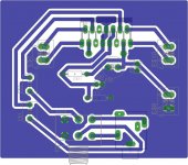
The attached photo shows the copper side of a small TDA7297 board (about 7*7 cm). What do you think about components placement? routing?
P.S: i realize that the input signal lines (from the input capacitors to chip pins 4 and 12) are a bit long but now i am too tunnel vision so i need your extra set of eyes.")
Thanks
The attached photo shows the copper side of a small TDA7297 board (about 7*7 cm). What do you think about components placement? routing?
P.S: i realize that the input signal lines (from the input capacitors to chip pins 4 and 12) are a bit long but now i am too tunnel vision so i need your extra set of eyes.
Thanks
Attachments
Thanks and sorry for the inconvenience.moved
Is it fine or is it not? come on guys, every opinion matters.
Not.
See how they have done it in the chips data sheet.
See how everything is routed.
Copy that basic design to your pcb software and then start improving...
Thanks for the reply but allow me a few questions...
Care to elaborate on that as i can't see any essential differences regarding routing and ground paths.
The layout in the datasheet is for application circuit Fig(1) where the mute and standby signal are coming from a microprocessor off board. What i am trying to build is the simple circuit in Fig(3) so there is a slight change in the component and i also added a dual pot for volume control. Aside from that what exactly do you see that could be a potential problem?
Not.
Care to elaborate on that as i can't see any essential differences regarding routing and ground paths.
See how they have done it in the chips data sheet.
The layout in the datasheet is for application circuit Fig(1) where the mute and standby signal are coming from a microprocessor off board. What i am trying to build is the simple circuit in Fig(3) so there is a slight change in the component and i also added a dual pot for volume control. Aside from that what exactly do you see that could be a potential problem?
Also saparate the chips power ground from its signal ground. Connect the chips signal ground to the audio ground.
Thanks for the advice, will do that.
Somehow separate the power ground from the audio ground, then connect them together in one point.
How would that go with the ground fill i am using? a jumper wire on the top layer?
Imade ultrafast design in 10 minutes or so, left stby...
how to screenshot on windows 7
Im not sure about the grounding, it might me noisy...
I didnt check what can happen if Signal GND is not connected to PWR GND...
An externally hosted image should be here but it was not working when we last tested it.
how to screenshot on windows 7
Im not sure about the grounding, it might me noisy...
I didnt check what can happen if Signal GND is not connected to PWR GND...
Last edited:
Remove the ground fill.
It increases parasitic capacitances that complicate your stability margins.
Thanks will do.
Imade ultrafast design in 10 minutes or so, left stby...
An externally hosted image should be here but it was not working when we last tested it.
how to screenshot on windows 7
Im not sure about the grounding, it might me noisy...
I didnt check what can happen if Signal GND is not connected to PWR GND...
Thank you but why did you use two capacitors for each supply (PWR) pin instead of only two for both pins?
This amplifier is probably not worth making...
The ground has extreme loop but not sure how will the chip act...
The supply rails are perfectly the same length and are connected together and arent long and thin, same with input and output rails...
But power rails arent that correct, if you connect wires straight from bridge rectifier then you may get mains noise on the output
The Vcc rails should go to capacitor and then to chip but they go to the chip before the caps...
There sould be connector for wire from supply GND to sig GND
Anyway, i got everything needed to build this amp, even stuff to make PCB...
Last edited:
This amplifier is probably not worth making...
The ground has extreme loop but not sure how will the chip act...
The supply rails are perfectly the same length and are connected together and arent long and thin, same with input and output rails...
But power rails arent that correct, if you connect wires straight from bridge rectifier then you may get mains noise on the output
The Vcc rails should go to capacitor and then to chip but they go to the chip before the caps...
There sould be connector for wire from supply GND to sig GND
Anyway, i got everything needed to build this amp, even stuff to make PCB...
Though i couldn't understand most of the post here are two questions:
1-Did you mean connecting signal ground to power ground through jumper wire?
2-Why did you use two capacitors per power pin (i.e four capacitors)?
Thanks.
Someone will soon come and tell you guys that the Mihkus PCB is a no-no, because everything related to the power supply and everything related to the audio circuitry must be kept as far away from each other as physically possible...
So, power in from the other side of the PCB and audio in from the other...
Audio ground you will connect to the power ground at the least noisiest point of the power ground. Jumper is good for the purpose or possibly even a small value resistor.
Also, by looking at the block diagram of the chip I am not sure if the ground fill makes much difference to the chips performance? I might be wrong though - I have absolutely no experience with the chip... I am a LME49811 guy... ;-)
Someone will soon come and tell you guys that the Mihkus PCB is a no-no, because everything related to the power supply and everything related to the audio circuitry must be kept as far away from each other as physically possible...
Agreed but it is a bit challenging in a 5cm*5cm single side board.
Audio ground you will connect to the power ground at the least noisiest point of the power ground. Jumper is good for the purpose or possibly even a small value resistor.
Thank you for the clarification
but by the "least noisiest point" do you mean close to the power ground entry point?Someone will soon come and tell you guys that the Mihkus PCB is a no-no, because everything related to the power supply and everything related to the audio circuitry must be kept as far away from each other as physically possible...
So, power in from the other side of the PCB and audio in from the other...
Audio ground you will connect to the power ground at the least noisiest point of the power ground. Jumper is good for the purpose or possibly even a small value resistor.
Also, by looking at the block diagram of the chip I am not sure if the ground fill makes much difference to the chips performance? I might be wrong though - I have absolutely no experience with the chip... I am a LME49811 guy... ;-)
Exactly. The design is rubbish I d rather choose TDA1519CTH, less useless things..
If you check Datasheet figure 3b... Just copy the damn thing and your done.
Exactly. The design is rubbish I d rather choose TDA1519CTH, less useless things..
What "less useless things"? the external components required by the TDA7297 and the TDA1519 are almost the same and i personally prefer the 7297 hence the thread.
- Status
- This old topic is closed. If you want to reopen this topic, contact a moderator using the "Report Post" button.
- Home
- Amplifiers
- Chip Amps
- TDA7297 Board Layout Suggestions