Gootee, let me try and make it more obvious that I am agreeing with you. A snubber has two critical parts right? A cap and a resistor? If either value is wrong the snubber ceases to perform its purpose. My cap is too small to snub the 14KHz resonance. After all caps DO snub. The difference is between snubbing and damping. It's a snubber and not a damper because it only damps resonances above the corner frequency. The cap's effect is to prevent damping frequencies that do not need damping, so that power is not wasted or linearity not compromised.
My damping resistor needs to be lower than 16R. How can I put this directly across the secondary without making a smelly heater or ozone destroyer?
BTW, thanks for the math info. I did not know that trick.
My damping resistor needs to be lower than 16R. How can I put this directly across the secondary without making a smelly heater or ozone destroyer?
BTW, thanks for the math info. I did not know that trick.
Kean, I don't think you are agreeing with Gootee.
The capacitor does not act as the snubber of the oscillation.
The resistor dissipates the oscillation energy. The resistor is the snubber.
As Gootee and many others have said the capacitor is only there to reduce the dissipation in the snubbing resistor.
That dissipation could be due to both DC voltage and AC voltage. When significant resistor dissipation is due to the AC voltage, then using the method of Haggerman, or of Gootee, you can determine the capacitor value to minimise the resistor dissipation.
The capacitor is there only to minimise the dissipation in the snubbing resistor.
A little word, or several, of caution.
The esr of the capacitor will dissipate some energy. If the esr dissipation is significant, then you are risking overheating of the capacitor.
Last edited:
A snubber is two components, not just one. A snubber acts as dampening within the frequency range. Without a capacitor it would not be a snubber. I would not call a lone resistor a snubber any more than I would call a lone capacitor a snubber. Yes, the resistor dissipates the resonance. But that is only half of the snubber. Like I said, without the cap I would be making a smelly heater or a watt to heat converter. The cap is no more optional than the resistor. As far as I know, a snubber is universally known as a series RC network. No, the cap does not damp, rather it prevents damping. But it does snub.
As long as we mean things the same way, it's only semantics how one calls it.
Still I'd prefer to stick to the common definition of a snubber as something that dissipates any out-of-band RF and spikes by applying a proper moderate resistive current path between two circuit points. This requires some resistance to act as the converter into heat, chosen to maximize the dissipation (drain away energy from the circuit). Since most often we have some wanted DC and LF content one needs the capacitor to isolate these signal components from the dirt, removing unwanted dissipation in the resistor.
Still I'd prefer to stick to the common definition of a snubber as something that dissipates any out-of-band RF and spikes by applying a proper moderate resistive current path between two circuit points. This requires some resistance to act as the converter into heat, chosen to maximize the dissipation (drain away energy from the circuit). Since most often we have some wanted DC and LF content one needs the capacitor to isolate these signal components from the dirt, removing unwanted dissipation in the resistor.
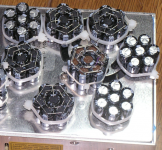
Did you use more than 7 caps parallel?
Sorry I'm a bit slow to join the party here, but your mention of 7 caps makes me want to share a pic with you guys. I wire up 7 caps in a hexagonal arrangement. This works best with caps which are the tall, thin kind in terms of optimizing ESR and ESL.
Also here's a paper about how LTPs on opamps introduce distortion in the presence of RF - I know both Daniel and Jay have extolled the sonic benefits of singletons in chipamps, this paper gives a plausible reason as to why.
Attachments
I have been doing a lot of reading on power supplies over the past few days, and now know enough to get myself in trouble (and a little embarrassed  ) by asking semi-informed questions.
What primarily come to mind are the two approaches, on-board vs. discrete, placement of the PS. I ask this question based on the excellent results achieved in the MyRef designs. From my level of understanding, just the parts count alone (Daniel's latest PMed PS version is ~32 components) presents two widely divergent approaches.
I understand the goal is simply to feed the actual amp stage(s) the cleanest and most stable power, and we really appreciate the "first things first" path the thread is taking. But, again with reference to the MyRef results, and the following comment from KSTR:
"Further, I'm not a fan of fully independent mono-blocks (even when in the same chassis), so a complete stereo PCB with most of the supply components on board seems more adequate for most builders I would think. For DIY we also have the option to make use of unorthodox layout/component placement as we do not need to care about feasibilty for mass production (which means sticking to all SMT parts located on the same side)."
Has the optimal PS location/seperation been definitively agreed upon? That is not totally clear to me. Does this need any further discussion?
) by asking semi-informed questions.What primarily come to mind are the two approaches, on-board vs. discrete, placement of the PS. I ask this question based on the excellent results achieved in the MyRef designs. From my level of understanding, just the parts count alone (Daniel's latest PMed PS version is ~32 components) presents two widely divergent approaches.
I understand the goal is simply to feed the actual amp stage(s) the cleanest and most stable power, and we really appreciate the "first things first" path the thread is taking. But, again with reference to the MyRef results, and the following comment from KSTR:
"Further, I'm not a fan of fully independent mono-blocks (even when in the same chassis), so a complete stereo PCB with most of the supply components on board seems more adequate for most builders I would think. For DIY we also have the option to make use of unorthodox layout/component placement as we do not need to care about feasibilty for mass production (which means sticking to all SMT parts located on the same side)."
Has the optimal PS location/seperation been definitively agreed upon? That is not totally clear to me. Does this need any further discussion?
The hexagonal cap bank is interesting. In this orientation the magnetic fields are aligned circularly like a toroid except for the center cap. I don't know whether this will improve magnetic interference but if the space around the cap has any effect on ESL than the effect here would be to increase it. I would orient the pins circularly instead of radially and connect the caps with twisted wires. This would minimize wiring inductance and the magnetic fields of the caps would cancel with them all facing inward (except again for the center cap).
I would think that the RF modulation effect would be worse for singleton frontends because they conduct better in one direction. I think it is misunderstanding the paper to say that it's just LTPs that suffer from this. An NTP (sibling of LTP) may have an advantage in that there is no parasitic capacitance to the rail at the summing point, but RF modulation may be worse because of the asymmetric conduction.
We can't know if we mean the same thing unless we get semantics right. There is no telepathy and guessing only leads to stumbling blocks. Without understanding each other we can only "agree to disagree" which is a crying shame when the problem is nothing but unclear semantics.
Abraxalito,
thanks for the paper, nice to see some emprical data.
Bob,
Please keep in mind that the MyRef, being a nested amp with a seperate local low voltage supply for the master opamp, is a bit different that a standalone wrt supply issues.
At any rate I'm open to discussion. Basically I could imagine design a supply concept that is quite open to different options for everyone's likings, ranging from completely isolated mono-blocks á la MyRef to the shared off-board main tank with only little local bypass. This kind of flexibility comes at a slightly higher cost (of the PCB, literally) and requires more design effort, in this case with the modified local bypass schemes and the series elements which are another playground for customization.
OTOH, now if there were some global preference for single-PCB mono-blocks here then let's zero in on those, perhaps with easy options for shared transformer (and diode bridges) to reduce cost/complexity for some builders.
Regulated front end, Nested, Composite & Howland (MyRef)
The MyRef apparently uses "regulated front end" model. The front end is the small signal op-amp. Regulated front end amplifiers can have power supply on same board as amplifier.
The series elements for the power supply of the MyRef front end power circuit are:
LM317, LM337. And the front end power caps are 100u.
(CQC, bigger voltage drop than CDC, but similar)
The series elements for the lm3886's onboard front end power circuit are:
PCB Traces, and then "re-stiffened" by 220u directly at the LM3886
(Mostly CLC, with a miniscule bit of CRC action)
Note:
Possible series elements include: Regulators, Transistors, Diodes, Resistors, Inductive cables, Inductors, and Inductive PCB Traces. And I propose that non-inductive or much less inductive series elements may be easier to control than inductor roulette. Since RF filtering turns up missing with non-inductive series elements, I proposed that the non-inductive series element (Regulators, Transistors, Diodes, Resistors) could be wearing an FB73 ferrite (or smaller) as a bracelet in order to restore/provide the filter function and still fairly predictable.
Large signal, high current area, Outputs:
It is usually pretty good to have some large capacitance available to the output devices for delivering bass impact. Caps for MyRef LM3886's output device power are 10,000u.
Last edited:
When not using "regulated front end"
The TDA7294 PCB's from Ebay, have hardwired the output and front end power circuits together. Just remember that the cleaner power needs of the front end have not changed, and we shall be needing a series element followed by a cap that can charge very fast, such as 220u.
Unfortunately, the "simple" PCB has the outputs siphoning from the front end's power circuit, which is a compromise--the entire board is front end (small signal) power circuit. Like the LM1875 chip, the one and only large signal (entirely output specific) connection is: speaker ground.
An effective series element is not included with purchase of the TDA7294 PCB; however, it could be a cable from amplifier board to power board. This is "normal" but unfortunately cables are inductors, and quite like a tuner coil, really dodgy to get it just right.
I propose that a non-inductive series element (Regulators, Transistors, Diodes, Resistors) could be easier to use and a lot more consistent so that everyone could be "on the same page" rather than suffering inductor roulette.
In comparison to the MyRef:
The simpler TDA7294 board didn't remove complexity. Omitting functions doesn't accomplish that (unless one is willing to accept decreased performance). These (unfilled) needs and their normal complexity was merely relocated. And that location is dc cables, layout and power supply board.
Front end power circuit MyRef and TDA7294 PCB compared:
MyRef front end power circuit has regulators for series element, followed by 100u.
TDA7294 front end power circuit has cable for series element, followed by about 220u.
In this comparison, the TDA7294 front end power circuit is suffering from a poorer quality series element and suffering from a heavier load since the output devices are also using the front end power circuit and it needs clean power no matter how much load it is supporting. So, for the TDA7294 PCB, a finer quality power supply board could be helpful.
Last edited:
Since the trafo resonance is in the audio band I wonder if a person could hook up a coil to their amp input and put it near the trafo. Then listen to the output, adjust snubber for cleanest hum.
There may be higher resonance modes requiring their own snubbers but I found snubbing the 14KHz resonance made the biggest impact on sonics. It would be interesting to try and address each individual resonance that could be found.
There may be higher resonance modes requiring their own snubbers but I found snubbing the 14KHz resonance made the biggest impact on sonics. It would be interesting to try and address each individual resonance that could be found.
What are your thoughts on running the TDA7294 from LM317/LM337, and having the TDA7294 push nice big discrete output devices?
At first glance, if we're considering any added parts, it seems good to improve linearity and current capacity, as would be suitable for driving a speaker.
At first glance, if we're considering any added parts, it seems good to improve linearity and current capacity, as would be suitable for driving a speaker.
Let me clarify a bit. I personally don't have a problem with what I called the "higher parts count"/off-board PS designs. If that method represents the fewest trade-offs for optimal performance of this specific chip, that's the desired way to go IMHO. I'm assuming KSTR (as the lead PBC maker for this project) has preferences that will allow him to escape the limitations of his commercial endeavors. I'm sure there are several PS designs that will work and work well. I just wasn't sure a consensus had been reached for a "no holds barred" PS development path.
The need for something between power for the existing eBay kits and the optimized developed board on this thread may or may not be necessary. There are a couple options/opportunities to pull a large number of potential participants from other threads that might influence that, based on cost and complexity.
At the moment I'm just trying to identify what will be used for the "top end" build.
Make sense ???
The series elements for the power supply of the MyRef front end power circuit are:
LM317, LM337. And the front end power caps are 100u.
(CQC, bigger voltage drop than CDC, but similar)
Sorry Daniel but the My_Ref has a simple zener shunt PS... one series resistor and one zener shunt per rail.
I was staring at this:Sorry Daniel but the My_Ref has a simple zener shunt PS... one series resistor and one zener shunt per rail.
http://www.diyaudio.com/forums/atta...on-rc-build-thread-my_ref_fe-rc-schematic.pdf
Actually, MyRef-FE.
I just checked again. The regulated front end features LM317 series elements followed by 100u. Looks like really good quality there.
I was staring at this:
(...)
Actually, MyRef-FE.
Exactly, it's my variation.
I just checked again. The regulated front end features LM317 series elements followed by 100u.
Those LM317s are CCSs, actually, and they replace the current setting resistors of the original My_Ref PS.
Also the shunt is improved by a shunt transistor that lower the zener impedance by transistor's HFE.
In fact the 100uF are completely optional, to the point they're left unpopulated in actual builds.
Looks like really good quality there.
Thanks
Bob, the PSU designs that I made are for supporting basic chip amplifier projects, such as TDA7294 board from e-bay.
This is definitely not optimal.
There's far too much room for unfortunate and confounding build variances that can make each build sound much different.
The MyRef people have it right with the all-in-one board Monobloc that reduces build variance (blocks errors) and avoids inductor roulette except for the transformer itself.
Conversely. . .
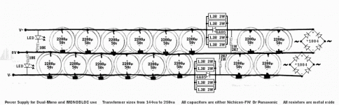
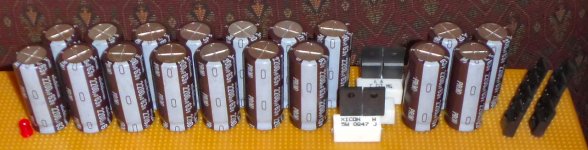
Attached is the reliable old gal from post #82, now dressed up in high heels and lipstick and ready to party with a monobloc. The collection of black & gold Nichicon-FW 2200u is not only pretty but can recharge very fast despite a plaster cracking bass beat (actually drywall, not tested with real plaster). If this power supply is set too close to an amplifier board, there's somewhat less chance of dulling than if we had used huge caps. Unfortunately, attempting to mitigate cable variances isn't very effective from the power supply end of the cable. SO, whatever DC cable is chosen can affect the needed capacitance size on the amplifier board and vice versa. When it comes to build variance, that's unpredictable performance causing each build to perform differently. I can't block this problem with a power supply board design, but you could block this problem with an amplifier board design.
This is definitely not optimal.
There's far too much room for unfortunate and confounding build variances that can make each build sound much different.
The MyRef people have it right with the all-in-one board Monobloc that reduces build variance (blocks errors) and avoids inductor roulette except for the transformer itself.
Yes, let's do that! Monobloc power and amplifier on one board allows you to choose series element much more predictable than a random cable, and Monobloc simplifies building because when one is built, it serves as a non-confusing point of reference.OTOH, now if there were some global preference for single-PCB mono-blocks here then let's zero in on those. . .
Conversely. . .
Attached is the reliable old gal from post #82, now dressed up in high heels and lipstick and ready to party with a monobloc. The collection of black & gold Nichicon-FW 2200u is not only pretty but can recharge very fast despite a plaster cracking bass beat (actually drywall, not tested with real plaster). If this power supply is set too close to an amplifier board, there's somewhat less chance of dulling than if we had used huge caps. Unfortunately, attempting to mitigate cable variances isn't very effective from the power supply end of the cable. SO, whatever DC cable is chosen can affect the needed capacitance size on the amplifier board and vice versa. When it comes to build variance, that's unpredictable performance causing each build to perform differently. I can't block this problem with a power supply board design, but you could block this problem with an amplifier board design.
Attachments
Last edited:
Thanks Daniel, that narrows down the options as required. I'm still planing to build the "reliable old gal" next week as I need the experience of doing so and want to determine hands-on what the audible differences are.
So Mr. K, can you give us your perspective relative to your board design plans?
So Mr. K, can you give us your perspective relative to your board design plans?
I needed a power supply with a bit higher voltage tolerance (for a discrete amp), so I'm making one too.I'm still planing to build the "reliable old gal" next week as I need the experience of doing so and want to determine hands-on what the audible differences are.
Those are the Fairchild Stealth II 16A 600V soft/fast schottky in the bridge rectifier. Almost slightly confusing to hook up. I'm glad the schematic has clearly marked KBPC1004's!
I'll probably redo the "CRC resistor" section. But it has 0.31R and that series pair of 16a fast silicon diodes has 0.9V forward voltage drop (and half the diode capacitance). Some more significant wattage non-inductive resistors is planned for an upgrade later; however, I'm using on-hand materials at the moment.
Anyway, you're looking at a rather fast 19,800uF per rail, in a monobloc's power supply.
The transformer is 400va in order to assure that this is still enough capacitance even if 4 ohm speakers are connected to the discrete amp (or parallel TDA7293 might could do it).
Attachments
Last edited:
- Status
- This old topic is closed. If you want to reopen this topic, contact a moderator using the "Report Post" button.
- Home
- Amplifiers
- Chip Amps
- Optimizing TDA7294 Output