Okay, if the shout went up, then the stability probably decreased. However, it is intensely unsuitable to use the decoupler size as the main stability control (we weren't taking cheap shots anyway). So, in the relevant case, what I said was that greater resolution may be achieved at the expense of greater stability labors (or a more convenient situation that didn't require as much compromise, like driving one rather tame tweeter).what is this supposed to mean?
Why don't you use normal technical english to explain what you claim the amplifier does when the "size goes down"?
Last edited:
If you care to look at the lm3886 datasheet you will see National's gain vs frequency and phase vs frequency plots.
I have not seen one for 1875, some of the others may have similar plots.
On that plot you will see what phase margin is available driving a resistive test load for the different gains one could choose.
If one were to choose the lowest recommended gain of 10times (+20dB) one would see the low phase and gain margins that come with that choice.
There is much anecdotal evidence that a gain of around +28db to +30db gives a nice sound quality.
Look at the plot. Gain = +28dB results in 82degree phase margin.
Again there is some expert opinion that around 80degrees phase margin is the optimum for a dominant pole amplifier.
The anecdotal evidence seems to match the expert opinion.
Set an lm3886 gain to +28dB for best sound.
There is no need to spout on about "shout"
Just use the appropriate technical language: say the gain and phase margins work well for good audio performance when the 3886 gain is +28dB. It need be no more complicated than that !
There is no need for your unfathomable descriptions that technically could mean anything and everything.
Last edited:
Well, this is a TDA7294 thread, and also we happen to talk about the TDA7293 which are less likely to be fake (so long as all 15 pins work). Therefore the TDA7293 is a recommended substitute for the purposes of this thread, and the TDA7293 datasheet is the relevant document. Except if one is really determined to use a fake TDA7294, in which case the TDA7296 datasheet is the relevant document.
There's also some talk about the amplifier board because most have bad layout, and that problem can be literally reduced by shopping for the very smallest board there is, so as to get the decoupling positioned closer to the voltage amp (pins 7 and 8).
And there's the usual caveat in that excessive power voltage causes additional compromise, resulting in a high power amp with at least one problem; so, instead of that, we have discussed making higher quality 40W~45W amplifiers.
That (derating) plus good layout and power, helps us get the gain down to 33x with the TDA7293, without further caveat.
With either more work at all parts of the circuit or far more derating, or both, it would be possible to set the gain even lower.
Last edited:
I couldn't figure that out. Does the TDA7293 datasheet have it?so what is the phase margin shown on the datasheet?
I am familiar with the national LM3886 chipamp. That datasheet does spell it out (the plot).
Is there any information on stability margins for your chipamp?
Without that you can only build an exact copy of the manufacturer's recommended build and then one should get the published performance.
Is there any information on stability margins for your chipamp?
Without that you can only build an exact copy of the manufacturer's recommended build and then one should get the published performance.
It wouldn't be as much fun if it were easy...
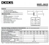
Ok, I get it that a resistor in series with a high current of up to 5amps and 25-30 volts is a tricky thing to spec. But I am not able to reconcile this with your prior endorsement of enhancing the filtering effect of the decoupling caps by using just the diode rectifier. My initial response was "why not complete the LPF that the capacitors are hinting at, with a series resistor?" A preliminary Low Pass Filter calculation calls for about 20k Ohms in order to create a low-pass filter at that location effective down to under 1Hz using the existing 450 uF of decoupling capacitance. I did take a look at the datasheet for the 6A05, and it specifies "Low Voltage Drop", so I'm having a hard time figuring out how the diode which I thought was primarily a check-valve, is now functioning as a resistor (which also varies with temperature).
Anyways - I'm happy to try it either way. I think I found some Ohmite resistors that can handle the current at that spot (may need a heatsink).
So here are two sketches - (variation on one of your schematics) One shows just the Diode, the other one shows a Diode plus a Resistor.
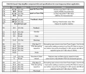
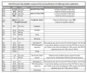
I'll follow this up with some BOMS that spell out where I am changing component values from one-amp to another to fine-tune frequencies to each driver.
Cheers! - Sixto
...I use diodes for that task (as indicated in my schematics)... it is my opinion that notion of series resistors on the rails, should be reserved for preamplifiers and other low current needs--definitely not power amplifiers.
Ok, I get it that a resistor in series with a high current of up to 5amps and 25-30 volts is a tricky thing to spec. But I am not able to reconcile this with your prior endorsement of enhancing the filtering effect of the decoupling caps by using just the diode rectifier. My initial response was "why not complete the LPF that the capacitors are hinting at, with a series resistor?" A preliminary Low Pass Filter calculation calls for about 20k Ohms in order to create a low-pass filter at that location effective down to under 1Hz using the existing 450 uF of decoupling capacitance. I did take a look at the datasheet for the 6A05, and it specifies "Low Voltage Drop", so I'm having a hard time figuring out how the diode which I thought was primarily a check-valve, is now functioning as a resistor (which also varies with temperature).
Anyways - I'm happy to try it either way. I think I found some Ohmite resistors that can handle the current at that spot (may need a heatsink).
So here are two sketches - (variation on one of your schematics) One shows just the Diode, the other one shows a Diode plus a Resistor.
I'll follow this up with some BOMS that spell out where I am changing component values from one-amp to another to fine-tune frequencies to each driver.
Cheers! - Sixto
Attachments

I'll follow this up with some BOMS that spell out where I am changing component values from one-amp to another to fine-tune frequencies to each driver.
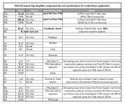
Here they are, preliminary values for each of the 3 amps: Low, Mid, High frequency. I've noted in bold the values that change from amp to amp, and their corresponding filter values (where I could calculate it)
I did not provide filter values for the FB-shunt because I could not figure out why when I try to calculate 1/2PiRC for even the Low-Freq amp (970 uF Fb-shunt, 730 r for multi-turn Pot) I get results like .22 Hz which seems too low, and would go even lower if I added-in the FB resistor value. Instead I simply reduced the capacitance of the Mid and Treble amps by the same ratio that the input filters are reduced. (using the lowest frequency of the bandpass range)
Curious to hear back what you all think. At this point, unless there are some glaring mistakes - I may just go ahead and start building and testing to see if I can hear the differences when I use different components. It will take time. (maybe by year-end?)
Thanks for all the advice so far, keep it coming! and remember I am such a newbie at this that it may take a few tries before things sink-in.
Sixto - Minneapolis
P.S. - here is a link to the TDA7293 Datasheet, it's mostly foreign to me, but maybe there's an answer to someone's question there? http://www.st.com/st-web-ui/static/active/en/resource/technical/document/datasheet/CD00001887.pdf
Attachments
Last edited:
With almost every chip having the same/similar generic schematic in the datasheet, despite the fact that the chips are all different, then it is not reasonable to assume that optimal values are shown in all cases. In the case of these ST datasheets the schematics are sketchy and partially hazardous; however, the graphs, text and tables are useful.Without that you can only build an exact copy of the manufacturer's recommended build and then one should get the published performance.
Last edited:
Those are confident conclusions !With almost every chip having the same/similar generic schematic in the datasheet, despite the fact that the chips are all different, then it is not reasonable to assume that optimal values are shown in all cases. In the case of these ST datasheets the schematics are sketchy and partially hazardous; however, the graphs, text and tables are useful.
Are you sure?
Oh yeah!Those are confident conclusions !
Are you sure?
It isn't good news. The power circuit has wrong size parts (overheat and ringing result), the bootstrap is slightly undersize with slightly increased chance of explode (correct size is 33u but they substituted a more convenient 22u), the rf filtering is lacking (what? was there an ink shortage?), the gain is low enough to get the amp a little nervous at the published voltage (if you had wanted to drive a speaker, that is), and the unnecessarily complicated mute circuit takes up so much space that the majority of board layouts position the decoupling ineffectively farther away from the chip. It is a lot of elementary errors, but the sum of that, is high risk of disaster. A lot of these chips do burn up because of following a generic schematic.
I worked hard on my TDA7293 schematic, to stay as close as possible to reasonable looking. Philfr worked hard on his LM3886 schematic, which is also reasonable looking, and quite similar. A considerable amount of your input went into both (in the form of goals to try for).
Both of these will, confidently, beat the datasheet generic schematic.
Last edited:
Can you give a link to the sch showing the component labeling?
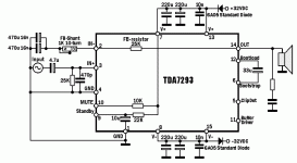
Yes, both schematic versions are attached to post #727. The only difference between them is the use of R6 and R8 at the power inputs.
Regards, Sixto
Thanks!
That reminds me to update the value printed on that trimmer, to something readable and also indicate that it could run as low as 33x gain, if built as indicated, at the voltage indicated and on a really tiny size board. Other usage may need higher gain for good stability; and as much as people like to mod, it is really good to have that trimmer. The trimmer also allows one to dial in the setting that the amp needs to run correctly, which won't ever be the same as the gain figure that one had in mind. Use of the dial provides the necessary evidence to defeat arbitrary notions, with the most likely end result of a well running amplifier.
That reminds me to update the value printed on that trimmer, to something readable and also indicate that it could run as low as 33x gain, if built as indicated, at the voltage indicated and on a really tiny size board. Other usage may need higher gain for good stability; and as much as people like to mod, it is really good to have that trimmer. The trimmer also allows one to dial in the setting that the amp needs to run correctly, which won't ever be the same as the gain figure that one had in mind. Use of the dial provides the necessary evidence to defeat arbitrary notions, with the most likely end result of a well running amplifier.
Attachments
Last edited:
Check valve function, and the "R" for a CRC, are both true. Remember that my amplifier is made with capacity for excellent bass power. Therefore the diode used for series element is a high current, low voltage, sort with the current versus voltage drop graph in the datasheet looking much like a straight up wall, and the minimal voltage variance is necessary for minimized sag--It covers a wide current range far more suitably than a resistor could do.I did take a look at the datasheet for the 6A05, and it specifies "Low Voltage Drop", so I'm having a hard time figuring out how the diode which I thought was primarily a check-valve, is now functioning as a resistor (which also varies with temperature).
It would be far too much work to change to a different resistor value for each different position of the volume knob.
Also, an actual resistor would eat your bass power by promoting sag; however, this difference is not relevant to a low current tweeter-only amp.
These series elements are positioned at the edge of the amplifier board, in which locale, cannot hinder the charge-up of the power supply reservoir.
The approach can be enhanced by applying various means of RF blocking (RC's, 3u polyester cap at rail to rail, or FB43 ferrites) at the spot where the DC umbilical cable has contacted the series diodes. That is probably also true of low current applications that have used resistors instead of the diodes shown. That is a great place to add additional RF filtering.
Hi Mark! Any idea what values I ought to use for that output RC?The diode works like a variable resistor. At low current the resistance is high and at high current the resistance is low. This has a lower power and voltage loss compared to simple resistor.
For a 100W into 8ohms Power Amplifier the R value could be around 0r1 to 0r2
For the front end of that same amplifier, the R could be around 20r to 40r
For a preamp, or crossover and similar use a value for R of 10r to 200r depending on the Vdrop acceptable and the current draw of the device.
I posted a half crossover with rCRCRC where the two R values were 165r to drop the main supply down to suit the jFET stage.
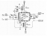
Feedback for low frequency driver/amplifier.
R1b is high, too much noise?
C6a & 8a seem very small.
Is that a datasheet recommended value?
I would (if the datasheet allows) fit 100nF to 220nF on the power pins and link them together with the shortest possible leads.
C6b,c &8b,c don't need to be split. Link this junction the the junction above. This is your Power Ground.
Just fit the biggest you can get fairly close to the chip, anywhere from 470uF to 1m5F
D6 and D8 serve no useful purpose as shown. They just drop useful voltage. The dynamic impedance of a diode is too low to make a useful high pass filter.
Change them to 1N4002, or higher and place them to link the output rail to the supply rails.
Add two more to link across the decoupling capacitors.
The Zobel does not help with capacitive loads. it is a high frequency load seen by the amplifier to help control gain at HF and thereby improve the stability margins.
If you want to add capacitive load tolerance you need to add an L||R between the output and the Speaker. Typically 1uH||10r but that 1uH is for a wideband amplifier passing upto 90kHz to the load. For mid, or bass duty it could be made higher value.
If the crossover is screened and the power amp is screened then external interference can't get in.
If all your signal connecting pairs are twisted then these limit internal interference . On that basis you may not need any input filters between the cross over and the power amp.
I don't know which of the chipamp ground pins is clean, or dirty.
I don't like the haphazard linking of all the signals to these unknown gnd pins.
I would separate the input signal (it is not GND, it is a two wire connection consisting of Signal Flow and Signal Return), from them completely and invoke HBRR. (IN-) and (IN+) are the signal input pins.
If you are wiring up as a non inverting amplifier then Signal Flow connects to (IN+) and Signal Return to (IN-) This is your arrangement. For inverting you would swap.
The NFB lower leg MUST connect to Signal Return, definitely NOT to the decoupling. Note that the internal upper leg NFB is already connected to (IN-).
Last edited:
- Status
- This old topic is closed. If you want to reopen this topic, contact a moderator using the "Report Post" button.
- Home
- Amplifiers
- Chip Amps
- Optimizing TDA7294 Output