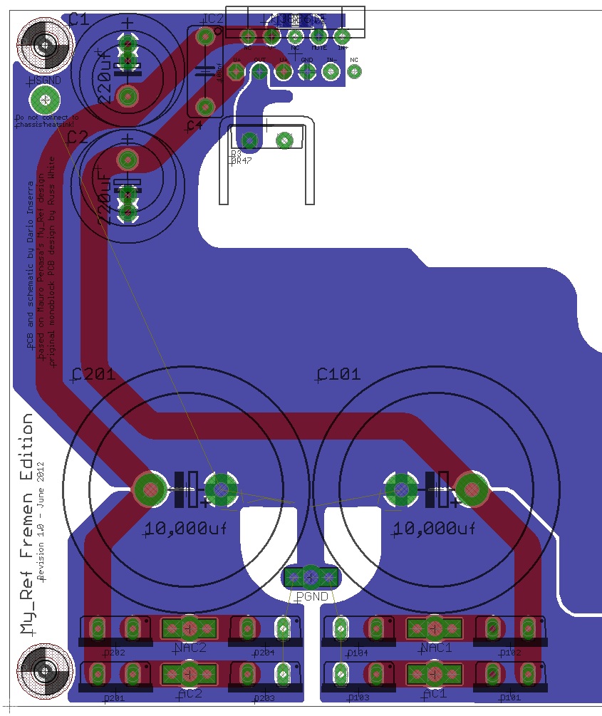
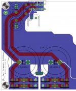
Yes, the output Zobel is located under C1.
A MELF resistor connecting at the output trace and crossing the V+ trace, and a 0805 capacitor.
I have marked it (blue rectangle) in the attached picture.
Is the placement ok?
I moved down the row of SMD parts for about 1.4mm, to make room for an alternative footprint for C9 (Cf).
Stupidly, I didn't find any SMD capacitors in the 50pF range other than ceramics (C0G or NPO).
So, if I want to use a foil type for Cf, I will have to pick a THT part.
But I could move the other parts back upwards, where they were before.
Would that be better?
I initially planned to use the unregulated CarlosFM design and read the whole thread about it.
But then I came across the explanations of Rainwulf here on page 65: http://www.diyaudio.com/forums/chip-amps/43423-high-cap-unregulated-psu-chipamps-65.html#post1761186
This sounds very reasonable for me, so I think I will follow these guidelines.
It's really-great to hear that you have seen the light, in Rainwulf's excellent post! If I remember correctly, everything he said was exactly accurate and he is thinking about all of that in exactly the right ways. His post was very gratifying to read, because I have been trying to emphasize almost the same points, over and over, in this forum.
One thing that I can see that might make a significant improvement, if changed, is the local reservoir (decoupling) capacitors' configuration. The suggestion is to change the PCB area they occupy, slightly, to basically make two power planes on one side of the board and a single ground plane on the other side, and populate them with many smaller caps instead of just two larger caps, while keeping the total capacitance about the same.
This would provide several significant benefits, including lower PSU impedance (perhaps much lower) as seen by the chip's power pins, at every frequency, as well as a type of averaging and redundancy that would make the circuit much more robust against future variations in capacitor parameters. It would also increase the lifespan of the capacitors, since a larger number of smaller ones will have more surface area than one larger one, for the same total capacitance, so they will run a little cooler. Also, with smaller caps, you will be able to get some of them even closer to the power pins, which should be one of the highest-priority goals, since it reduces the inductance and resistance of the connections. (And even if you DON'T switch from one large cap to many smaller ones, you should STILL try very hard to get at least a few smaller electrolytics MUCH closer to the power pins.)
Just thinking out loud about paralleling caps: If you used n caps in parallel, even if they were all n times farther away than the original single larger cap, you could, roughly, still divide the total inductance and resistance each by n, and would have n times as much as each one's capacitance, while also NOT increasing the total conductor self-inductance or resistance at all! That would be wonderful but it gets even better. Since the n caps are each much smaller than a single large equivalent-value cap, it's extremely likely that the average connection length would be significantly LESS than n times as long, for n capacitors. So the total connection self-inductance would also be significantly reduced. i.e. There is no "downside", only significant benefits, piling on top of each other.
Actually, the same should be done for the power supply reservoir caps, which should basically be right next to the amp, too, if possible.
There is a guy named Terry Given, an extremely-bright electronics and electromagnetics engineering professional, whom we are very lucky to have on Diyaudio, who expounded on this, a while back, and also gave some brilliant yet very practical DIY construction methods (and numbers/measurements to back them up). I will try to post links to the most-relevant posts. Sorry there are so many but the result is a simple but brilliantly-better capacitor configuration.
http://www.diyaudio.com/forums/power-supplies/216409-power-supply-resevoir-size-101.html#post3154192
http://www.diyaudio.com/forums/power-supplies/216409-power-supply-resevoir-size-101.html#post3154202
http://www.diyaudio.com/forums/power-supplies/216409-power-supply-resevoir-size-102.html#post3154705
http://www.diyaudio.com/forums/power-supplies/216409-power-supply-resevoir-size-102.html#post3155158
http://www.diyaudio.com/forums/power-supplies/216409-power-supply-resevoir-size-103.html#post3155261
http://www.diyaudio.com/forums/power-supplies/216409-power-supply-resevoir-size-103.html#post3155293
http://www.diyaudio.com/forums/power-supplies/216409-power-supply-resevoir-size-103.html#post3155415
http://www.diyaudio.com/forums/power-supplies/216409-power-supply-resevoir-size-121.html#post3166558
http://www.diyaudio.com/forums/power-supplies/216409-power-supply-resevoir-size-122.html#post3166773
I do wish there were more of us ( and I include me in there) that have seen the light in local decoupling.
Unfortunately we are massively outnumbered by Members that won't think about the problem they embed into their PCB layouts. And worse, refuse to alter their layout when told of the poor practice they use. Why do they refuse to alter: "because it always works for me"
There is another just as important topic that is getting more airing. Small Loop Areas.
Design for small loop areas in the whole amplifier, be it an opamp, or discrete line driver, or a big power amp.
Last edited:
The two grounds are already separated by a resistor (R8) and two anti-parallel diodes (D1, D2). The connection point is located in the lower right corner, right from the output terminal, and under the input connector.
Now I see it! Fine
")
Interesting, as I think about it, I'm more concerned about the Zobel resistor picking up noise from the V+ trace and leading it back to the feedback input.
What about if I rotate the Zobel by 90°, so that it would go downwards instead of left?
I think it would be better.
Ok, I will cut the plane over the output trace.

Sure, but I wonder why such low-value capacitors are not available as SMD.
I think, especially these are predestinated for SMD, to get rid of the influences of the terminal legs.
But for example the ECHU series is available from 100pf on.
They're available... from Mouser (MC12 1210 size SM)
Regarding LM3886 decoupling I would use LM3886 pads as vias so that you sit the decoupling caps on the groundplane.
Attachments
Last edited:
I do wish there were more of us ( and I include me in there) that have seen the light in local decoupling.
Unfortunately we are massively outnumbered by Members that won't think about the problem they embed into their PCB layouts. And worse, refuse to alter their layout when told of the poor practice they use. Why do they refuse to alter: "because it always works for me"
There is another just as important topic that is getting more airing. Small Loop Areas.
Design for small loop areas in the whole amplifier, be it an opamp, or discrete line driver, or a big power amp.
I have, for a very long time, counted you among those who truly do understand and appreciate the importance of those ideas, and was very glad that you did because you have been an untiring educator. Bravo, AndrewT.
As I think you know, minimizing enclosed loop area has been somthing that I, too, have tried to emphasize, here, over and over. Loops enclosing geometric area are antennas, both receiving and transmitting. The two worst places to have them are probably in the AC transformer and rectifier areas (transmitting), and in the sensitive signal input interconnct and amplifier input areas (receiving). Two-sided PCBs make it so simple to eliminate them in the pcb-mounted parts of a system but even then, a lot of people either don't know about it or just don't realize the critical importance of it.
Keep plugging away at them. I can't even count the number of posts I've written, trying to stress better layout techniques for minimal loop area, proper star grounding, and better decoupling capacitance configuration (and RF filtering; can't forget that).
Maybe someday I will make the time to try my ideas for hand-made multilayer PCB stacks. That would at least provide us with dedicated whole PCB layers for power and ground rails. The main key idea there is just that we would need to drill relatively large access holes, to be able to have solder joints on inner layers (and maybe also wherever "pass-throughs" were needed). It would require a bit different type of layout planning and PCB design than we do, now. But it would also give us much more freedom when designing the layout, and should eliminate a lot of potential worries, while giving almost the best-possible performance that a hand-made PCB could give.
Suddenly I'm envisioning two interspersed sets of many parallel electrolytics covering the "bottom" side, to implement a "Terry Given Super-Low-Impedance Decoupling Capacitor Array", which could be tapped-into directly at the power pins of every active chip or device, anywhere on the top side.
Or, we could forget the multi-layer stuff above and instead just try to figure out how to be able to get two cap-array boards mounted close-enough to the chipamp power pins, and connected in such a way that we don't ruin the low impedance.
The caps could be relatively small values, and the array could probably be fairly small, in terms of its board size. So maybe it wouldn't even be too difficult. I'm thinking of a 10 x 10 (or larger) array of something like 100 uF to 470 uF (for each cap in the array). Those caps could each be quite small. But how could we get the edge of their board to be right at a chipamp power pin? Maybe the cap-array pcbs would have to be vertically mounted near the bottom of the chipamp pcb, right under the chipamp.
Cheers,
Tom
Thanks at all for the very valuable hints you gave, I really appreciate that!
That whole power supply topic with all that considerations should really be worth a "sticky"!
So everybody can think about it before actually designing a PCB (especially those which don't want to discard anything they've already painted in their layout software).
I will do some planning to implement that the best way I can...
For local decoupling, there was planned one Elna RJH 470µF per rail, with 12.5mm diameter.
For that diameter, the greatest capacitor value I could find was a Panasonic FR 820µF with about three times better values in ripple current capability and impedance.
The next smaller diameters are 10mm with a maximum capacity of 270µF, and 8mm with a maximum capacitance of 180µF.
So to get the originally planned capacitance, I would have to use 2x270µF or 3x180µF.
I'll see if I can get that properly aligned next to the power pins...
For power supply decoupling, I originally planned to use 10,000µF per rail, Panasonic TS-HA (35mm) and Elna LAH (30mm) looked the best, each with about 4A ripple current rating and ESR of 0.033.
To "array-ify" that, I would need 10x1,000µF (16mm) or 5x2,200µF (18mm).
Wow, this will get huge, compared to the originally planned size...
That whole power supply topic with all that considerations should really be worth a "sticky"!
So everybody can think about it before actually designing a PCB (especially those which don't want to discard anything they've already painted in their layout software
).I will do some planning to implement that the best way I can...
For local decoupling, there was planned one Elna RJH 470µF per rail, with 12.5mm diameter.
For that diameter, the greatest capacitor value I could find was a Panasonic FR 820µF with about three times better values in ripple current capability and impedance.
The next smaller diameters are 10mm with a maximum capacity of 270µF, and 8mm with a maximum capacitance of 180µF.
So to get the originally planned capacitance, I would have to use 2x270µF or 3x180µF.
I'll see if I can get that properly aligned next to the power pins...
For power supply decoupling, I originally planned to use 10,000µF per rail, Panasonic TS-HA (35mm) and Elna LAH (30mm) looked the best, each with about 4A ripple current rating and ESR of 0.033.
To "array-ify" that, I would need 10x1,000µF (16mm) or 5x2,200µF (18mm).
Wow, this will get huge, compared to the originally planned size...
Well, sometimes I read of making the local decoupling as big as possible.
My thoughts about it were to provide a relatively big local reservoir with low ESR and high ripple current rating.
So I would get better impulse stability before the big (and farther away) reservoir capacitance at the rectifier board can deliver current.
And of course, they fit physically just right onto the PCB.
So you think I can reduce the local decoupling without having a guilty conscience?
Well, sometimes I read of making the local decoupling as big as possible.
My thoughts about it were to provide a relatively big local reservoir with low ESR and high ripple current rating.
So I would get better impulse stability before the big (and farther away) reservoir capacitance at the rectifier board can deliver current.
And of course, they fit physically just right onto the PCB.
So you think I can reduce the local decoupling without having a guilty conscience?
Maybe Andrew was only finding out how you selected the value.
More capacitance (or maybe even as much as possible) COULD be better. But low impedance at the power pins is the actual goal. And capacitance is only one component of that, here. Connection lengths will add inductance and resistance. Using one larger capacitor usually gives more inductance and resistance than using several smaller ones in parallel.
Seems to me the best way would be to use the largest number of parallel capacitors that still give enough capacitance, and get all of them as close to the power pins as you can. (I would try to get three of them really close, and then keep adding more, even though they would have to be farther away.)
You could assume that you will have way more than enough capacitance, and that you will do the best-possible job placing and paralleling them so that the inductance and resistance are as low as they could possibly be. That way, you wouldn't need to calculate the minimum required decoupling capacitance or the maximum allowable inductance and resistance, because if you didn't already meet the requirements there wouldn't be anything you could do about it anyway!
But if you don't want to get extreme about adding lots of parallel caps, then you might want to do some at-least-just-ballpark calculations. On the other hand, you could just "wing it", with an educated guess, and see what happens. (And I'm not necessarily implying that's a terrible idea.)
If you do just guess, then I would probably suggest going with at least three smaller caps in parallel instead of one larger-valued one.
Cheers,
Tom
Ok, I see the point.
My idea of getting one "the biggest value that fits onto the board"-capacitor was before your hint about parallelisation.
I just did some quick calculations with the Panasonic FR series:
without modifying my PCB, I could fit 4 pcs with each 6.3mm diameter per rail, instead of one with 12.5mm.
The biggest available capacity with 6.3mm diameter is 56µF, with 0.405A ripple current rating and impedance of 0.14 Ohm (inductance values are not stated in the datasheet).
So if I would parallel 4 of them, I would get 224µF with 1.62A ripple current and 0.035 Ohm impedance.
The corresponding value as a single cap is 220µF, with 1.65A ripple current and 0.03 Ohm impedance.
My originally planned capacitor had 820µF, with 3.27A ripple current and 0.014 Ohm impedance.
The (calculated) ESR values are: 2.368 Ohm for a single 56µF cap, which results in 0.529 Ohm for 4 paralleled caps.
The 220µF cap has 0.603 Ohm, and the 820µF has 0.162 Ohm.
Hmm, doesn't look too good for the paralleled capacitors in matters of impedance...
ESR is slightly better for parallel compared to single cap with equal capacitance, but the biggest cap is ahead here too.
So the crucial point must be inductance, otherwise using parallel caps would be quite senseless...
Are my calculations wrong, or have I missed something important?
Regards, Stefan
Yeah, you missed two things. But they're really one thing. Inductance and the distance from the pins. If you used multiple smaller caps in parallel, it is assumed that would mean that they could be much closer to the pins than would be possible with one larger cap. And even if they were not closer, since the inductance of the connections would be much greater than that of the caps, the multiple parallel caps would be significantly better (assuming their connections are separate-enough from each other.
The inductance is what kills you, at higher frequencies (which includes fast-changing transients), where it will dominate the impedance, compared to the resistance due to ESR + connection length.
You can estimate the cap inductance pretty well by using 1 nH per mm, times the lead-spacing in mm. And you can estimate the self-inductance of a trace or wire with the same figure, for now. You could also try looking at an even larger number of even smaller caps.
But look at the links I posted, at least once. You could chop off the part of your PCB with the big caps and replace it with a separate 1mm-thick 2-sided PCB, maybe 48 x 48 mm. Keep one side solid copper, for ground. Divide the other side in two, by removing copper to from one slot along the diagonal. DON'T make any traces or remove any other copper, except as described. Lay out positions for 15 8 mm caps on each half (rows with 5, 4, 3, 2, and 1 cap). Drill one hole per cap, for the lead that goes to the bottom side. Remove a little copper from around each hole, on the top side. Bend the top-side lead flat against the copper and solder. One end of the diagonal "slot" will go near the chip. Connect the power pins' traces from there, with something thick or wide. Connect the rails from the PSU to the opposite corners, at the other end of the diagonal slot.
That's only one possible topology. Also, using a larger number of even-smaller caps should be even better.
Sorry I couldn't explain any of that in more detail. I have to get up early.
Thanks, that was exactly the information that was missing in the datasheets!You can estimate the cap inductance pretty well by using 1 nH per mm, times the lead-spacing in mm. And you can estimate the self-inductance of a trace or wire with the same figure, for now.
As I said, I didn't find any suitable information about inductance, so I just calculated the values I could (ripple current, impedance, ESR).
But now I can clearly see that inductance will be much lower.
Here are the inductance values (just for the leads, traces are omitted here):
56µF has a 2.5mm pitch, so lead inductance will be about 2.5nH.
With 4 of them, that results in 0.625nH.
220µF and 820µF both have 5.0mm pitch, which results in 5.0nH.
So the parallel version is by factor 8 lower than a single cap with same capacitance, quite impressive.
Then I think I'll go with the paralleled version.
May I - or should I even - then omit the small foil bypass caps at the chip's supply pins, and still maintain optimal performance?
I'll try to implement a configuration like you described.You could chop off the part of your PCB with the big caps and replace it with a separate 1mm-thick 2-sided PCB, maybe 48 x 48 mm. Keep one side solid copper, for ground. Divide the other side in two, by removing copper to from one slot along the diagonal. DON'T make any traces or remove any other copper, except as described. Lay out positions for 15 8 mm caps on each half (rows with 5, 4, 3, 2, and 1 cap). Drill one hole per cap, for the lead that goes to the bottom side. Remove a little copper from around each hole, on the top side. Bend the top-side lead flat against the copper and solder. One end of the diagonal "slot" will go near the chip. Connect the power pins' traces from there, with something thick or wide. Connect the rails from the PSU to the opposite corners, at the other end of the diagonal slot.
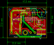
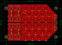
I have just made a new version of the rectifier board.
Both versions are equipped with dual rectifiers with 16K/W heatsinks per diode, bleeding resistors and space for diode snubber RC.
They have 2 outputs per rail (for stereo usage), and a third GND terminal for safety ground connection (via safety loop breaker).
My original version used a single 10,000µF capacitor per rail and provided space for a small film bypass cap.
(power planes have not been drawn, layout just for size estimation)
The new version uses 12x 820µF per rail and power planes on both sides.
Please ignore the thin lines around traces and pads, they are just clearance marks in KiCad.
Attachments
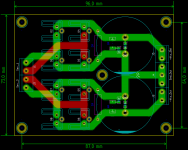
I've made for you a PS only version of my board to illustrate some concepts:
- keep diodes traces as simple as possible, try to avoid overlaps
- after smoothing caps try to keep V+ and V- traces paired on the ground plane, it will have an effect similar to twisting cables
- power traces on the groundplane have constant impedance if they mantain their width constant
- power traces on a groundplane will have a greatly reduced inductance (circa 40% less)
- When using groundplanes take in account current returns, HF current will follow power traces, LF will seek the least impedance path.
- Avoid slots in groundplanes, particularly on the current return path
- Sometime, though, slots are useful to isolate sections of the groundplane (see the small slots on the smoothing caps to sepate diode's plane from the general one)
- when routing traces avoid 90° angles, they will cause impedance changes and reflections that can possibly smear the signal.
- it's unlikely that those diodes will ever need an heatsink...
- do not remove the bypass caps on V+ and V-, use R2R bypassing if you want.
Attachments
Yes, I agree. Do not remove the small bypass caps. Could allow high-frequency instability.
SirPA,
Now you are getting the idea!
But the best performance should come from the easiest-possible layout: NO traces. One board for one power rail. Double-sided PCB. One side power and one side ground. All you need is a drill.
Or, I suppose you could use one board with one side ground plane and the other side could be split into two (+ and -) power planes.
ClaveFremen is right about not having a large gap between the + and - power rails, too. Enclosed loop area = antenna.
What you are doing is almost identical to what is described in the second half of post $1214, here: http://www.diyaudio.com/forums/power-supplies/216409-power-supply-resevoir-size-122.html#post3166773
And here is some VERY good news about a similar setup: http://www.diyaudio.com/forums/power-supplies/216409-power-supply-resevoir-size-103.html#post3155293
(like, you could get about 1 nH or TOTAL inductance, for ALL of the caps AND their "wiring"!)
And here are some construction secrets: http://www.diyaudio.com/forums/power-supplies/216409-power-supply-resevoir-size-102.html#post3155158
And here's much of the real story, probably about $20000 of consulting, all in one free post: http://www.diyaudio.com/forums/power-supplies/216409-power-supply-resevoir-size-102.html#post3154705\
It basically started here, which also has some key points: http://www.diyaudio.com/forums/power-supplies/216409-power-supply-resevoir-size-101.html#post3154192
It seems to me that we should simply use two capacitor arrays to connect the rectifiers to the chipamp power pins. (At that point, THEN you can remove the small bypass caps. <grin>)
Cheers,
Tom
Last edited:
Thanks!I've made for you a PS only version of my board to illustrate some concepts:
two additional notes:
- keep diodes traces as simple as possible, try to avoid overlaps
- after smoothing caps try to keep V+ and V- traces paired on the ground plane, it will have an effect similar to twisting cables
- power traces on the groundplane have constant impedance if they mantain their width constant
- power traces on a groundplane will have a greatly reduced inductance (circa 40% less)
- When using groundplanes take in account current returns, HF current will follow power traces, LF will seek the least impedance path.
- Avoid slots in groundplanes, particularly on the current return path
- Sometime, though, slots are useful to isolate sections of the groundplane (see the small slots on the smoothing caps to sepate diode's plane from the general one)
- when routing traces avoid 90° angles, they will cause impedance changes and reflections that can possibly smear the signal.
- it's unlikely that those diodes will ever need an heatsink...
- do not remove the bypass caps on V+ and V-, use R2R bypassing if you want.
I will try to implement that, as far as I haven't done yet, and where ever possible.
Regarding the diode heatsinks: The datasheet states that above ca. 3.5A, a heatsink is required.
For getting 60W@4 Ohm loudspeaker output power, a current of about 3.9A will flow. And for 2*20W@4 Ohm, even 4.8A.
I know the average power consumption will be quite less, but you never know.
So I thought it would be wise to include at least the option of a heatsink.
How warm do your diodes get, when you hear music a little louder?
Regarding the diode traces: Thanks for the hint, I've overlooked that! I could reduce it to exactly one crossing at 90°, if I swap the pins at the input terminals.
Because of that, I thought of omitting the 100nF film caps at the chip's power input pins, I thought they could perhaps even provide the possibility of HF instability.Yes, I agree. Do not remove the small bypass caps. Could allow high-frequency instability.
...
And here is some VERY good news about a similar setup: http://www.diyaudio.com/forums/power-supplies/216409-power-supply-resevoir-size-103.html#post3155293
(like, you could get about 1 nH or TOTAL inductance, for ALL of the caps AND their "wiring"!)
But I will leave them in place.
Sure, this would be the absolute optimum.Now you are getting the idea!
But the best performance should come from the easiest-possible layout: NO traces. One board for one power rail. Double-sided PCB. One side power and one side ground. All you need is a drill.
Or, I suppose you could use one board with one side ground plane and the other side could be split into two (+ and -) power planes.
It seems to me that we should simply use two capacitor arrays to connect the rectifiers to the chipamp power pins. (At that point, THEN you can remove the small bypass caps. <grin>)
But, as far as I could follow the "Power supply reservoir size" thread, it was referred to discrete power amps, with power stages consisting of perhaps multiple paralleled output transistors.
Connecting that to a massive cap array will be much simpler than a single (and comparatively small) all-in-one chip.
Because the other parts have to be connected to the chip in an optimal way, too.
Exactly from that post I took the inspiration for the PS board, although my approach isn't as good.What you are doing is almost identical to what is described in the second half of post $1214, here: http://www.diyaudio.com/forums/power-supplies/216409-power-supply-resevoir-size-122.html#post3166773
In that post, there is a lot interesting about SMT caps.And here's much of the real story, probably about $20000 of consulting, all in one free post: http://www.diyaudio.com/forums/powe...er-supply-resevoir-size-102.html#post3154705\
And, if I get it right, it would be the best to use the smallest case size possible to not ruin all efforts made so far.
But film caps are only available in 1210 case or bigger.
So wouldn't it be better to use a X7R ceramic in 0603 instead of film?
Hmm, to close the gaps, I would have to use Faston tabs for the transformer connections.ClaveFremen is right about not having a large gap between the + and - power rails, too. Enclosed loop area = antenna.
But somehow I don't quite like these, because of the tension stress for the PCB.
A few years ago I have seen Faston tabs with a molded plastic support base, to provide a bigger contact surface for the PCB.
That would have been ideal, but unfortunately I don't find them anymore...
Regards, Stefan
Thanks!
I will try to implement that, as far as I haven't done yet, and where ever possible.
You're welcome, Stefan.
Regarding the diode heatsinks: The datasheet states that above ca. 3.5A, a heatsink is required.
(...)
How warm do your diodes get, when you hear music a little louder?
They never get hot to the touch.
BTW the heatsink wouldn't harm.
Regarding the diode traces: Thanks for the hint, I've overlooked that! I could reduce it to exactly one crossing at 90°, if I swap the pins at the input terminals.
Hmm, to close the gaps, I would have to use Faston tabs for the transformer connections.
???
BTW the fastons I use are solidly bonded to the PCB (better if soldered on both sides) and are mechanically really strong...
Thanks!
I will try to implement that, as far as I haven't done yet, and where ever possible.
Regarding the diode heatsinks: The datasheet states that above ca. 3.5A, a heatsink is required.
For getting 60W@4 Ohm loudspeaker output power, a current of about 3.9A will flow. And for 2*20W@4 Ohm, even 4.8A.
I know the average power consumption will be quite less, but you never know.
So I thought it would be wise to include at least the option of a heatsink.
How warm do your diodes get, when you hear music a little louder?
Regarding the diode traces: Thanks for the hint, I've overlooked that! I could reduce it to exactly one crossing at 90°, if I swap the pins at the input terminals.
Because of that, I thought of omitting the 100nF film caps at the chip's power input pins, I thought they could perhaps even provide the possibility of HF instability.
But I will leave them in place.
The film caps actually might cause HF instability, if they happen to resonate with some inconvenient value of inductance, such as that of a large electrolytic. You are correct that X7R ceramic should be safer, there, in that sense. But if you have an oscilloscope, you could try the film caps and just check, under various conditions (square waves might be a good test, for that). The bottom line is that you need to have a low impedance at high frequency, there, between the pin and ground. How you acheive that doesn't matter to the high fequencies themselves.
Sure, this would be the absolute optimum.
But, as far as I could follow the "Power supply reservoir size" thread, it was referred to discrete power amps, with power stages consisting of perhaps multiple paralleled output transistors.
Connecting that to a massive cap array will be much simpler than a single (and comparatively small) all-in-one chip.
Because the other parts have to be connected to the chip in an optimal way, too.
Well I didn't say it would be trivial to figure out how to make it optimal. <smile>
And I haven't found a "perfect" way to do it yet, either. But here are some more spur-of-the-moment thoughts about possible methods and configurations:
The dual-triangular-arrays idea (which was just off the top of my head at the time) "might" work OK, since it gets two of the corners of the two triangles to end up near the same place that your original layout had the power traces going to the chip.
OR, maybe more likely to work well, you could have two rectangular arrays on one board and have them taper down somewhat, as they approach the chipamp area.
But I'm also thinking that maybe a more-three-dimensional solution could be better. Maybe a cap-array board parallel to the amp board. Or maybe two of them, with one above and one below (possibly like a "card cage", or, using standoffs). Then drop some large low-inductance conductors directly to the chip pin areas on the amp board, with power and ground.
You could also consider using card-edge connectors (like the old-fashioned type of PC motherboard card slots), with the card-edge connectors mounted on a "motherboard" PCB that contained ONLY power and ground planes running between the card-edge connectors, in order to run those between the cap-array boards and the chipamp board. You would use multiple connector "fingers" for each plane. i.e. The cap and amp PCBs' edges would have two (cap arrays) or three (amp board) solid copper areas that slid into the connectors and each solid copper edge-area would contact multiple fingers inside the card-edge connector.
I still like the idea of building-up a multi-layer PCB, from single and double-sided PCBs. Imagine not having ANY power or ground traces to worry about, in your layout, but having all of those available everywhere on the board, almost exactly where needed.
Exactly from that post I took the inspiration for the PS board, although my approach isn't as good.
It's good. Just remember that there is a big advantage in keeping the planes solid, i.e. unbroken, as much as possible, all the way to the point of load if possible.
In that post, there is a lot interesting about SMT caps.
And, if I get it right, it would be the best to use the smallest case size possible to not ruin all efforts made so far.
But film caps are only available in 1210 case or bigger.
So wouldn't it be better to use a X7R ceramic in 0603 instead of film?
The 0603 size should be better than the 1210, in terms of inductance. And that should then be better overall. But if you implement and connect the cap-array planes fairly well, the SMT caps would probably just be like a little extra dab of icing on an already-very-good cake, unless you were doing a digital circuit that had fast edge times. I could be wrong about that, though.
Hmm, to close the gaps, I would have to use Faston tabs for the transformer connections.
But somehow I don't quite like these, because of the tension stress for the PCB.
A few years ago I have seen Faston tabs with a molded plastic support base, to provide a bigger contact surface for the PCB.
That would have been ideal, but unfortunately I don't find them anymore...
Regards, Stefan
Eliminating gaps, to minimize enclosed loop area, is extremely important, too. I haven't looked at your transformer configuration so I can't comment on that. But it sounds like ClaveFremen has provided a viable solution for you.
Thanks, good to know.They never get hot to the touch.
I'll keep the heatsinks as an option.
Ok, maybe my bad experience was, because I used them on a home-etched single side PCB.BTW the fastons I use are solidly bonded to the PCB (better if soldered on both sides) and are mechanically really strong...
On a double side PCB with plated holes they will hopefully be much more robust.
Btw, I just found Faston tabs with bended stabilizers on the top side, I think I will use these.
Unfortunately I don't have an oscilloscope or other tools that might come in handy (as for example a network analyzer).The film caps actually might cause HF instability, if they happen to resonate with some inconvenient value of inductance, such as that of a large electrolytic. You are correct that X7R ceramic should be safer, there, in that sense. But if you have an oscilloscope, you could try the film caps and just check, under various conditions (square waves might be a good test, for that). The bottom line is that you need to have a low impedance at high frequency, there, between the pin and ground. How you acheive that doesn't matter to the high fequencies themselves.
So I'll better use a ceramic type here.
I already thought of something similar, using dual row pin strips (multiple pins for each rail) to sit the amp board on top of the rectifier board.Well I didn't say it would be trivial to figure out how to make it optimal. <smile>
And I haven't found a "perfect" way to do it yet, either. But here are some more spur-of-the-moment thoughts about possible methods and configurations:
The dual-triangular-arrays idea (which was just off the top of my head at the time) "might" work OK, since it gets two of the corners of the two triangles to end up near the same place that your original layout had the power traces going to the chip.
OR, maybe more likely to work well, you could have two rectangular arrays on one board and have them taper down somewhat, as they approach the chipamp area.
But I'm also thinking that maybe a more-three-dimensional solution could be better. Maybe a cap-array board parallel to the amp board. Or maybe two of them, with one above and one below (possibly like a "card cage", or, using standoffs). Then drop some large low-inductance conductors directly to the chip pin areas on the amp board, with power and ground.
You could also consider using card-edge connectors (like the old-fashioned type of PC motherboard card slots), with the card-edge connectors mounted on a "motherboard" PCB that contained ONLY power and ground planes running between the card-edge connectors, in order to run those between the cap-array boards and the chipamp board. You would use multiple connector "fingers" for each plane. i.e. The cap and amp PCBs' edges would have two (cap arrays) or three (amp board) solid copper areas that slid into the connectors and each solid copper edge-area would contact multiple fingers inside the card-edge connector.
But unfortunately this will only work for mono or dual-mono configurations.
Powering two amp boards from one rectifier board (as intend to use it for small output power) will not be possible, at least it will be far more complicated.
I have, for earlier projects, already thought of homebrew multilayer PCBs.I still like the idea of building-up a multi-layer PCB, from single and double-sided PCBs. Imagine not having ANY power or ground traces to worry about, in your layout, but having all of those available everywhere on the board, almost exactly where needed.
But it will be quite complicated.
One would have to use 1x 0.5mm double-sided base material and 2x 0.5mm single-sided base material.
Then one must think of placing all vias in an appropriate place, and how the inner layers can be contacted.
And that will be quite tricky and prone to errors.
One could also think of ordering the 3 PCB parts from a PCB manufacturer and laminate them at home.
But most pooling services only provide standard thickness of 1.6mm, and for the extra cost of the thinner base material there won't be much difference from ordering a 4 layer PCB...
I am just reworking the power supply board to close most of the gaps.Eliminating gaps, to minimize enclosed loop area, is extremely important, too. I haven't looked at your transformer configuration so I can't comment on that. But it sounds like ClaveFremen has provided a viable solution for you.
The transformer will be a dual secondary type.
Center-tapped toroids are hardly available, I think because dual secondary is more versatile.
Regards, Stefan
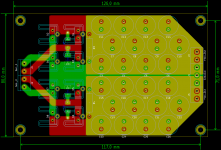
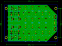
I've just completed the changes to the power supply layout.
Transformer inputs are now Faston tabs between the diodes, just like ClaveFremen proposed.
And the power planes have been closed, too.
As a nice side effect, the width decreased also by 11mm.
Red is top layer, green is bottom layer.
Transformer inputs are now Faston tabs between the diodes, just like ClaveFremen proposed.
And the power planes have been closed, too.
As a nice side effect, the width decreased also by 11mm.
Red is top layer, green is bottom layer.
Attachments
<snipped>
I have, for earlier projects, already thought of homebrew multilayer PCBs.
But it will be quite complicated.
One would have to use 1x 0.5mm double-sided base material and 2x 0.5mm single-sided base material.
Then one must think of placing all vias in an appropriate place, and how the inner layers can be contacted.
And that will be quite tricky and prone to errors.
One could also think of ordering the 3 PCB parts from a PCB manufacturer and laminate them at home.
But most pooling services only provide standard thickness of 1.6mm, and for the extra cost of the thinner base material there won't be much difference from ordering a 4 layer PCB...
<snipped>
Regards, Stefan
Stefan,
To get to the inner layers, you could just drill large holes in the other layers, as needed. You could use holes that are something like 5 mm in diameter, or more, so you could solder down inside of them, without having solder touch the in-between layers. With a multi-layer PCB-layout software package, it should be simple-enough to plan and execute such a layout correctly.
But if you were going to have a professional PCB fabricator make boards for you, then you should probably use a "real" mutli-layer layout and PCB.
Cheers,
Tom
I've just completed the changes to the power supply layout.
Transformer inputs are now Faston tabs between the diodes, just like ClaveFremen proposed.
And the power planes have been closed, too.
As a nice side effect, the width decreased also by 11mm.
Red is top layer, green is bottom layer.
I can hardly wait to hear about the results...
- Status
- This old topic is closed. If you want to reopen this topic, contact a moderator using the "Report Post" button.
- Home
- Amplifiers
- Chip Amps
- LM3886 component selection