I am building an LM3386 based stereo chip amp and I am trying to decide whether to wire point to point or use PCB.
I can etch PCBs but I hate doing it, and so far I can see that the only advantage to PCBing this amp, due to its simplicity, is for looks, with point to point even offering some advantages if done well due to keeping lead lengths nice and short and minimising stray capaticance.
What are your thoughts? Is it just a matter of personal taste?
Its a matter of personal taste. Point to point is easier to tweak the SQ of - I find grounding/decoupling schemes have a big influence on sound and tweaking that on a PCB is less convenient.
Myself I use a kind of hybrid between PCB and point-to-point. I buy a standard assembled PCB and hack it around because there's a fair amount of time to be saved in getting a functional amp module to begin with. The end result looks much worse than either of the two methods you mentioned though - its 'quick and dirty'
Myself I use a kind of hybrid between PCB and point-to-point. I buy a standard assembled PCB and hack it around because there's a fair amount of time to be saved in getting a functional amp module to begin with. The end result looks much worse than either of the two methods you mentioned though - its 'quick and dirty'
+1 ...Point to point is easier to tweak the SQ of - I find grounding/decoupling schemes have a big influence on sound and tweaking that on a PCB is less convenient.
Frank
P2P is perfect for small amp project like single 3886 in standard config.
Just make sure the the chip's leads are not stressed and bent to avoid any shorts between them. This I find most easily done by supporting the passive components with isolated stand-off eylet strips or turret boards like have been used in tube gear for decades (hint for purchasing). I often use a small central solid copper ground plane and buss bar. For quick prototyping I just solder everything together based on a piece of copper sheet, though.
With short, properly twisted and shielded cabling of critical connections the electrical properties of a P2P build can be outstanding. One might need shielded overall metal case for lowest hum and highest noise immunity.
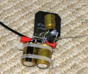
I took short signal paths to the extreme with my P2P 3886. Just make sure you don't want to change anything later if you go to that extreme.
I'd love to reduce the gain on mine but the thought of trying to replace the gain setting resistors has stopped me from doing it (If you have seen the pictures on my blog you will know why )
Tony.
I'd love to reduce the gain on mine but the thought of trying to replace the gain setting resistors has stopped me from doing it
(If you have seen the pictures on my blog you will know why ) Tony.
I'm going to disagree.
The 5pin chipamps really do suit P2P.
But only if you have already decided exactly which components are needed and what values each of them need to be. P2P is quite difficult to swap out later.
With the 3886 there are many extra pins that need extra components and there always seems to be less space than you want/need for the last component.
The 11pin chip makes even more important that you know exactly what components are needed.
I would suggest developing the final schematic on plug boards and/or on ready made PCBs, BEFORE you adopt the final P2P.
Last edited:
Andrew is partly right, I would say.
With P2P one still should decide whether you just prototype things in a temporary build, just soldering up things one some GND plane, or whether you go build "production quality units" -- or at least something that is nice and sturdy. But once you gonna make more than 3 units a PCB seems to be less effort (or effort shifted to the layout stage).
With P2P, the bypass and local supply capacitors tend to get in the way. One can extend the wiring to supply/bypass caps, though. I regularily use up to 10cm (4in.) of coaxial cable (75R satellite antenna cable) wired to blank double sided copper PCB strips with rows of capacitors soldered along the edges. This is as low inductance as it gets for the frequencies of interest (<20Mhz).
As I said earlier I went to extremes. Bypass and local supply caps are right on the chip pins, BUT it makes it very difficult to fit everything else in, and there is zero chace of changing anything later if so desired
I was a bit worried about temps for the feedback cap (the one on top of the chip) but I used a large heatsink and it only gets warm.
Tony.
I was a bit worried about temps for the feedback cap (the one on top of the chip) but I used a large heatsink and it only gets warm.
Tony.
Attachments
Last edited:
Extremes ... ?? Looks just about right to me, except I used about 12x that capacitance for local decoupling. Doing this "silly" stuff is exactly what gives one the extra, and significant lift in performance, if that is what one is after.As I said earlier I went to extremes. Bypass and local supply caps are right on the chip pins, BUT it makes it very difficult to fit everything else in, and there is zero chace of changing anything later if so desired
AFAIC, ordinary construction will always just give you ordinary sound ...
Frank
KSTR yes it works fine, though I ended up going back to my 100W mosfet amp because it handles my speakers better (4 ohms dipping as low at 2.7ohms at around 200Hz). The chip is ok at low volumes but falls apart if pushed, I suspect the protection circuit cutting in.
I built it in Oct 2005, mainly as a speaker testing amp, but it served as the main amp in my system for at least a couple of years It is currently having a rest
edit: Frank, it seemed extreme to me compared to the other P2P 3886's I was able to find pics of. At the time I built it I couldn't find any examples at all!
Tony.
I built it in Oct 2005, mainly as a speaker testing amp, but it served as the main amp in my system for at least a couple of years
It is currently having a rest edit: Frank, it seemed extreme to me compared to the other P2P 3886's I was able to find pics of. At the time I built it I couldn't find any examples at all!
Tony.
I can etch PCBs but I hate doing it
Well, don't do it then, this is a hobby, you're supposed to be having fun.
so far I can see that the only advantage to PCBing this amp, due to its simplicity, is for looks
Not so. The principal advantage, even with a simple design, is that the likelihood of errors in construction is lessened. If the schematic is drawn right, the PCB will be right, at least in terms of connectivity. This won't stop you inserting polarized components reversed, but I've corrected far more wiring errors on breadboards, perfboard and P2P layouts than on PCBs.
To err, they say, is human.
In my example I used that minimal lead length concept, with thick copper ground and power planes, which had very generous local decoupling applied. That was linked back to an OTT regulated power supply, which had ample energy reserves.KSTR yes it works fine, though I ended up going back to my 100W mosfet amp because it handles my speakers better (4 ohms dipping as low at 2.7ohms at around 200Hz). The chip is ok at low volumes but falls apart if pushed, I suspect the protection circuit cutting in.
I built it in Oct 2005, mainly as a speaker testing amp, but it served as the main amp in my system for at least a couple of years
edit: Frank, it seemed extreme to me compared to the other P2P 3886's I was able to find pics of. At the time I built it I couldn't find any examples at all!
Tony.
This all meant I had no problems whatsoever with "falling apart", easily kept up with and surpassed a commercial (older) 200W "hulk" amplifier. Only protection symptoms were thermal overload, a sustained pure tone by a soprano at full volume caused overheating, and the Spike circuit to cut in, like digital mistracking ...
Frank
Last edited:
Yes, but that can be overcome by improving heat extraction techniques and/or paralleling chips. After all, it's only trying to protect itself, from flagrant abuse ...Yeah the SpiKe protection of the LM3886 was the main reason I eventually ditched it in favour of the TDA7294 in a commercial application many years ago. Sounds dreadful.
Frank
I'd forgotten the 3886 only mutes and doesn't go into STBY, good point Klaus Out here the TDAs are under half the price of the LMs so there's really no competition. LMs do really score on comprehensiveness of data though - PSRR, CMRR, gain vs freq info is scant to non-existent for the TDAs. Oh and the isolated package option must count for something.
Out here the TDAs are under half the price of the LMs so there's really no competition. LMs do really score on comprehensiveness of data though - PSRR, CMRR, gain vs freq info is scant to non-existent for the TDAs. Oh and the isolated package option must count for something.- Status
- This old topic is closed. If you want to reopen this topic, contact a moderator using the "Report Post" button.
- Home
- Amplifiers
- Chip Amps
- LM3386: point to point or PCB?