Why are there only disastrous PCB Versions for TDA7293/TDA7294/LM3886 etc. available?
There are an extremly wide range of PCBs and Kits available for this and similar other monolitic audio amp ICs.
For me unfortunately the position of the copper conductor tracks are absolutely
disadvantageous by all examples, which are to find by Google image search - go to
audio amplifier tda7293 - Google Search
audio amplifier tda7294 - Google Search
lm3886 - Google-Suche
By this high resolution example - go to
F200# Audio Enthusiasts DIY AMP TDA7293 Amplifier Board for sale
you will see, that the positive voltage supply rail and the negative rail goes very close to the signal pads and inverted input pad for NFB. Additional there are only cheap caps for the power supply in use without screw terminals. Consequently a certain standart of sonic quality cannot be exceeded. By all showed images unfortunately this situation I note.
I am almost certain, that nothing of the showed versions from image-search sounds really good (at best like Linn's LK85 in genuine condition - i. e. with original part and wire equipment).
After performed tweacking of Linn's power amp model LK85 (equipped with TDA7294V) I observe an exceptionally enhancement by sound quality due to additional use of caps with screw terminals and change the routing of the wires for the main voltage rails.
According to my requirements four holes would be drilled in the PCB near by the pins 13 and 15 in case of TDA7293/TDA7294 (in opposite of the sensitive area). The cans of the caps must go downward (solder side/bottom side) and the screws for the caps must be screwed from the component/top side.
Then I avoid interchanges between the (very short) supply rails to the sensitive areas and I get the possibility to use top class capacitors in outlines like that from
http://www.audiocap.co.uk/ekmps/shops/audiocap/images/als30a153ke063.gif
or
http://s.eeweb.com/resized/images/r.../2011/02/15/vishaycaps-1297787376_455_332.png
instead low cost high CV versions in "snap in" outline.
Are such printed circuit boards really still not available ??
If yes, is this unbelievable. OTOH - there are too many copies of copies (clones of clones), particularly in far east.
Where is the excellent engineering from early days concerning proper PCB design ??
Attachments
Last edited:
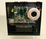
As long supply rails to find close to the sensitive areas PCB design is for me clearly desastrous.As for XY LM3886 kits, I do not know if this PCB can be considered as desastrous or not though the sound is five stars as is, i.e. no mods.
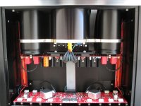
Here an other example in the right direction; Jeff Rowland's wiring diagram of Concentra/Concentra II and Model 10 looks interesting
Jeff Rowland LM3886 Amplifiers
hifi-advice.com
Attachments
Last edited:
I suppose it should only be considered "Disasterous" if the curcuit self-destructs or at the very least sounds like crap , but a lot of PCB"s don"t follow every rule of proper PCB design and work just fine and sound just fine .....
The PCB in the TDA7293 Datasheet isn"t a particularly well designed PCB (though is was odviously designed by an engineer) but the PCB works and sounds just fine ......
I suppose to some poeple it is more important that a PCB follow all proper conventions of PCB design than the actual performance of the PCB ......
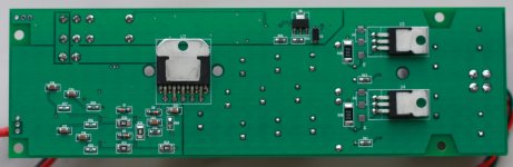
If making the PCBs, why not make 'em better?
Anyone else got a good chipamp pcb/schematics examples?
tiefbassuebertr, i'm laying-out some lm3886 right now, this one (latest published) -
http://s3t.it/data/uploads/lm3886v5.jpg
The trimpot is next to opamp right now.
http://s3t.it/data/uploads/lm3886_v4.pdf
LM3886 regulated u-Gainclone
This one is wrong too? (criticism is welcome)
The whole point of doing a PCB is sothat the circuit works as designed, everything else is secondary, though if the PCB cannot be made then its a pointless exercise. The elctrical functionality always comes first if the board is being designed properly, and the main skill in PCB layout is component placement, get that right and all else follows.I suppose to some poeple it is more important that a PCB follow all proper conventions of PCB design than the actual performance of the PCB ......
For chipamps layout is not as critical as it is for SMPS's and Class D amps, now there you can see some disasterous layouts.
How close is close? If the supply is well filtered and doesn't have a lot of noise on it, and if the capacitance and leakage between the traces is low, there shouldn't be any problem. Phase also matters. Can you define a rule for length and distance that divides acceptable and unacceptable?
I don't know 'bout other ICs, but LM3886 has it's output/PS pins nicely aligned pretty far from it's input. That should be the least distance between high-current and low-current nodes.
Yet, keeping the PS rails close to ground/each other has more significance than extending the distance between high-current and low-current nodes.
/imho/
Yet, keeping the PS rails close to ground/each other has more significance than extending the distance between high-current and low-current nodes.
/imho/
For low level analogue a minimum of 3W where W the general track to track spacing, and the basic track width, this allows a guard track between the two signal traces.
The best way if forthe engineer to put this information onto (or better still built in) to the schematic.
When doing sensitive audio (or other analog designs) I use different trace codes for different signals, usually "mic" for low level, "line" for higher level signalsand so on, the engineer draws the schematic using the defined codes, then when you lay the board out you can see the different signals in pretty colours defining the different types of signals. So you dont route a mic trace near a line traceor use more space betweenthe different signals to avoid cross talk and other interference.
For digital the same basic rules apply, but for sensitive digitalsignals such as clocks, also on digital I have various EMC advisores and simulation toolsthat we can use to checkthe whole layout.
Indeed - this looks good. Thank you for this URL.
http://www.s-audio.com/wp-content/uploads/2008/12/zd-50-rev-d712107-main-board.pdf
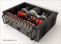
read post #1 (LK-85, Linn)Why do you think so?
For low level analogue a minimum of 3W where W the general track to track spacing, and the basic track width, this allows a guard track between the two signal traces.
The best way if forthe engineer to put this information onto (or better still built in) to the schematic.
When doing sensitive audio (or other analog designs) I use different trace codes for different signals, usually "mic" for low level, "line" for higher level signalsand so on, the engineer draws the schematic using the defined codes, then when you lay the board out you can see the different signals in pretty colours defining the different types of signals. So you dont route a mic trace near a line traceor use more space between the different signals to avoid cross talk and other interference.
For digital the same basic rules apply, but for sensitive digitalsignals such as clocks, also on digital I have various EMC advisores and simulation toolsthat we can use to checkthe whole layout.
This is a very good approach in order to avoiding layout errors.
Attachments
Last edited:
Forgot to mention:
You can set up spacing classes and rules in higher end tools, which further constrain layout and again helpavoid errors.
I also use a two screen setup so that the schematic isalways open and with the cross probing function I can see on both the layout and the schematic which component or trace I am playing with.
Setting all the rules and spacing classes before you start a layout save tears after.
Maybe the new tool fromForgot to mention:
You can set up spacing classes and rules in higher end tools, which further constrain layout and again helpavoid errors.
I also use a two screen setup so that the schematic isalways open and with the cross probing function I can see on both the layout and the schematic which component or trace I am playing with.
Setting all the rules and spacing classes before you start a layout save tears after.
Announcing OrCAD 16.6?A One-Two Punch for Mainstream PCB Engineers
helps additional.
Unfortunately I don't master its handling.
Actually I want to have tools for circuit design like LT-spice or circuitmaker, which comprehend all parasitic components like all spread inductors and capacitors between the tracks.
But to avoid crosstalk from the supply rails to the sensitive areas, it is only necessary to create solder/srew areas for screw-in caps but without traces. Put on a twisted pair of leads, which faces away from the PCB i do not regard as a serious issue.
This is dependend of the kind of error. If one create an unwanted capacitor between the output and the inverted input (input for NFB), e. g. by intersecting traces, you will get an oscillator instead an amplifier.The whole point of doing a PCB is sothat the circuit works as designed, everything else is secondary, though if the PCB cannot be made then its a pointless exercise. The elctrical functionality always comes first if the board is being designed properly, and the main skill in PCB layout is component placement, get that right and all else follows.
For chipamps layout is not as critical as it is for SMPS's and Class D amps, now there you can see some disasterous layouts.
Last edited:
Used Orcad in the past and PADS, but have mainly used the Cadstar suite over the last zillion years. All the good packages will allow you to set design rules, not so critical for simple designs, but when you are doing a mainly analogue board 50mm x 80mm with 1900 pins (SMD) and 1500 connectionsit becomes a necessity.
Orcad is quite ghard to get to grips with and set up, it took me 3 months before I was fully happy with the set up and comfortable using the software.
Orcad is quite ghard to get to grips with and set up, it took me 3 months before I was fully happy with the set up and comfortable using the software.
I suppose it should only be considered "Disasterous" if the curcuit self-destructs or at the very least sounds like crap , but a lot of PCB"s don"t follow every rule of proper PCB design and work just fine and sound just fine .....
The PCB in the TDA7293 Datasheet isn"t a particularly well designed PCB (though is was odviously designed by an engineer) but the PCB works and sounds just fine ......
I suppose to some poeple it is more important that a PCB follow all proper conventions of PCB design than the actual performance of the PCB ......
I don't understand this term:
"...and work just fine and sound just fine"
If I have heard before the sound from a flat screen television or lapptop I get the impression of a fine sounded device.
If I have heard before the sound from a very fine amp and very find speaker (very fine chain) the same device with same sonic character sounds very bad at once.
Please note: the better part is the enemy of a good part.
For me a disasterous layout is still present, as long I don't get the best possible results due to non perfect conductor truck guide arround the PCB. Particularly in such cases, where such PCBs in very expensive amp devices are in use.
Last edited:
With LM3886'ish & TDA7294'ish chips, the important things are that you have clean behaviour up to about 10Mhz (except for output pin snubbers, 50Mhz) and get the grounding and bypassing right. Then some care about loop areas and high impedance nodes and you're set, assuming a properly designed and tested schematic.
As of yet I've seen only one commercial chipamp offer which was plagued by massive supply hum from visually "nice" but electrically disaster layout. Many other designs (also in active speakers) might be on a "just OK" level. But there are for sure excellent chip amp variants around which is not only a question of layout/wiring...
As of yet I've seen only one commercial chipamp offer which was plagued by massive supply hum from visually "nice" but electrically disaster layout. Many other designs (also in active speakers) might be on a "just OK" level. But there are for sure excellent chip amp variants around which is not only a question of layout/wiring...
Last edited:
I don't understand this term:
"...and work just fine and sound just fine"
If I have heard before the sound from a flat screen television or lapptop I get the impression of a fine sounded device.
If I have heard before the sound from a very fine amp and very find speaker (very fine chain) the same device with same sonic character sounds very bad at once.
.
Maybe I"m not blessed with golden ears and am not a HiFi guy (build mostly guitar amps) but I have designed mic preamp PCB"s where my main obejective was only to get connections and components correct with very little redard to "Best Practices" and had them be very successfull , most of the mic preamps in my studio were built on half arsed one off single sided PCB designs and they sound as good as or better than my comercial pre-amps , at least to my untrained ears......
The only rules that i follow is to try to keep supply traces away from signal traces , seperate audio and power grounds and to put local decoupling as close to the chips as possible .......
Maybe the avoidance of PCBs is the best solution - go to
http://www.diyaudio.com/forums/chip...t-no-pcb-tda7293-tda7294-tda7295-tda7296.html
Looks very good - at least at first glance.
http://www.diyaudio.com/forums/chip...t-no-pcb-tda7293-tda7294-tda7295-tda7296.html
Looks very good - at least at first glance.
Last edited:
Perhaps the middle ground between point to point versus PCB?
For kit boards, the easy three step solution is to:
1). Put the feedback resistor trackside, onto the chip pins.
2). Relocate the nanofared power bypass cap to the chip pins.
3). Stand up a 2.2R (or more) small signal groundlift resistor in any one of the bus ground spots and then hook all the small signal ground shunts and the input cable ground to the top of that resistor, thereby lifting most of the small signal up off the kit board.
- Home
- Amplifiers
- Chip Amps
- Why are there only disastrous PCB Versions for TDA7293/TDA7294/LM3886 etc. available?