good advices. Additional important from my view it is to divert a twisted line for the supply rails upward or downwards from the PCB but in no case conductor traces therefore on the PCB itself (except very short ones to the srew holes for electrolytic caps).Perhaps the middle ground between point to point versus PCB?
For kit boards, the easy three step solution is to:
1). Put the feedback resistor trackside, onto the chip pins.
2). Relocate the nanofared power bypass cap to the chip pins.
3). Stand up a 2.2R (or more) small signal groundlift resistor in any one of the bus ground spots and then hook all the small signal ground shunts and the input cable ground to the top of that resistor, thereby lifting most of the small signal up off the kit board.
Amplifier board power caps.
It is also possible to install an identical sample of the "main" cap, such as 330u or 220u electrolytic as your NFB cap, proceed to bypass it attractively (the goal is to avoid peaks), and then use copies of that setup for the amplifier board power caps. Sure, that's not perfect by ear; however, avoiding resonant peaks is a considerable improvement.
I'll bet you didn't want 100n for bypass!
I wouldn't want to blame the PCB layout for the schematic error of "arbitrary bypass" with guaranteed wrong values causing ringing.
Probably a 1u or smaller size electrolytic will do a nice job in bypassing a 330u or 220u electrolytic. However, 1u electrolytic on both rails at the audio amp might be a bit disturbing, since the centerpoint between the two caps is also the reference for inverting input. I really don't want to input all that. Therefore I used one of lossy polyester cap of 2u from rail to rail. This lossy cap is internally R-C-R (possibly a real RCR works?). Successful application makes for less congested and clearer midrange, and possibly a slightly cooler heatsink. Rail to rail cap doesn't attach to 0v and therefore it doesn't contact small signal input.
In either case above, the task of bypassing the 330u or 220u amplifier board power caps is mostly done. Now I can select range from 0.47n to 10n bypass caps to finish the job. These are so small that they don't taint the audio like peaky 100n arbitrary bypass error.
Probably my explanation is terrible, but what I hope to convey is this:
If a given bypass doesn't work for small signal then it doesn't work for power circuit either. Integrating a big cap with a smaller cap requires the same careful precision as integrating a woofer with a tweeter (and careless non-specific use makes a similar peaky mess). Successfully good power circuits have obvious audio benefits, such as the clear and level sounding response of decreased distortion. Arbitrary bypass is a schematic error, not a PCB error. I suggest to mail all of the 100n to the North Pole and then try for less peaky bypass methods. I believe that the PCB's will work better with non-ringing power circuits.
Gosh, I hope that helps. Probably the PCB layout designers weren't expecting the ringing caused by typical schematics. Those criss-cross mixup boards are expecting, totally clean, flat DC. And, I believe that expectation is invalidated by most schematics.
Last edited:
are there additional new knowledge and experience in the meantime??
In this case also this thread could be of interest:
http://www.diyaudio.com/forums/chip-amps/226437-optimizing-tda7294-output.html
In this case also this thread could be of interest:
http://www.diyaudio.com/forums/chip-amps/226437-optimizing-tda7294-output.html
Last edited:
Mad pinout problem solved by Compact double-layer board
No problem! Drum roll please. . . Introducing, non-disaster TDA7294 and non-disaster TDA7293:
TDA7294
TDA7294 65W Mono Amplifier Board Kit 28 | eBay
TDA7293
1pc x TDA7293 Mono Amplifier Board Official Standard 85 w Original B Board | eBay
Parallel TDA7293
1 PCX Assembled Finished 170W TDA7293 2 Dual Parallel Mono Power Amplifier Board | eBay
(for 4 ohm speakers)
P.S. I'm not endorsing the component values or components on these boards; however, I do like the double-layer PCB. As the datasheet recommends, the mute circuit is overly complex. And, these boards don't have small signal groundlift feature. But those are minor issues that are easily corrected. The boards do still offer very short trace length and I think that's a useful feature for supporting these particular chips.
P.P.S. If you want a non-disaster LM3886, then I think you're looking for the MyRef-FE.
Last edited:
But you can assume, that companies like SGS-Thomson or NS (now TI) goes completely different ways for reach perfect results than small audio companies for getting good results at their PCB routing layout.Kind of silly considering we have no control over the package pins/ bond wires/ routing and layout of the die. Like the $10000 line cord not accounting for the wires inside the walls.
Thus your statement is nonsense (except if the chip amp devices are fakes from China).
Kind of silly considering we have no control over the package pins/ bond wires/ routing and layout of the die. Like the $10000 line cord not accounting for the wires inside the walls.
That's the point.
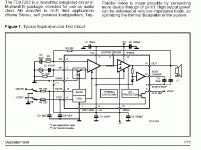
Pin layout of TDA7293/4 is stupid crazy, the designers bring internal connections whick *must* be joined, to non contiguous legs. Stupid.
Pin7>13 and Pin8>15

Why didn't they spend 5 minutes more rerouting the *internal* layout , or even better joining said points *inside*.
Worst case, they could do it the hard way, adding the necessary couple wires at the die itself, before encapsulating.
This complicates PCB design, of course, and , as Art M correctly says, nothing the PCB designer does will change that.
On the contrary, LM3886 pin assignation is very good
Whoa!?!?
It's the reason the TDA could be better than the LM - it has SEPARATE input and output stage supply pins, which is great.
I wish the LM had these.
Its possible to get the output modulating the input if the output and input supplies are not seperated.
Whoa!?!?
It's the reason the TDA could be better than the LM - it has SEPARATE input and output stage supply pins, which is great.
I wish the LM had these.
Well, it "could" ...
but since everybody uses them joined ... even the datasheet example , I stick to my opinion.And anyway, even if that was the original idea, they still might have used contiguous pins, so both options are easy to choose.
As is, it unnecessarily messes with the PCB layout.
In both cases they have not 1 or 2 but 5 or 6 legs in the middle.
If course, *she* also thinks that crisscrossing those tracks is no big deal:

Attachments
Last edited:
That's a good reason to go double-layer PCBs and reconsider the tradeoffs of trace length, inductance and current loops.
danielwritesbac,
I hope you've forgot to put quotation marks across the "non-disaster" idiom
These eBay PCBs are Good examples of Bad Layout
The main, heaviest current path is between the output stage rails, TDA's output and GND pins of bypass caps. This region should be as small loop area as possible.
What do we see on eBay (and lots of other PCBs)? The supply comes 'round the left/right edges of the board. Huh.
Bypass caps, as close to the IC as possible? Nah, they are subminiature and placed at the farthest place possible - on the opposite corners of PCB.
They are laid out for:
- Small overall footprint
- Cool/simple connectors placement
- Smallest bypass caps, because they are pricey
Yet, i have to say, they did a Great Job on cost reduction front. 10$ for 50w of power, shipped?
Well, it "could" ...
[/IMG]
I don't join them !
It is wrong to just join them and that is lazy and cheap design.
Its the same with random earthing of a layout and then wondering why you get hum.
PCB designs is a bit of a black art and get it wrong and your audio sounds like !"!££"$£
non disaster design
An externally hosted image should be here but it was not working when we last tested it.
chriscam,
Your's PCB looks nice, especially given the restrictions of 3-channel design. What are the board dimensions? I'm thinking of something similar, but with 6 channels and 10x10cm PCB
But i may drop the 6-channel thing and go 3-4 channels if 6 won't fit.
There is a nice feature for multiway amplifiers - they don't need to be precise copies of each other - especially on power supplies. You can feed the most powerful channel with main large caps, and then feed the other channels with RC filter where R will limit the current and C would be calculated for the xover cutoff frequency. This way you get most of the power on the woofer, and delicate and clean supplies on mid/tweeter. Not to mention the reduced bypass cap sizes for mid/tweet section.
300Hz and 1ohm resistor = 680uF caps
2000Hz and 1ohm resistor = 100uF caps
These are tiny!
Last edited:
Your's PCB looks nice, especially given the restrictions of 3-channel design. What are the board dimensions?
Thanks
 it's 100mm x 80mm, double layer with DC protection, 8000uF onboard buffer.
 An externally hosted image should be here but it was not working when we last tested it.
An externally hosted image should be here but it was not working when we last tested it.
It's accompanied by a 3ch substractive 12dB xover, mfb correction & limiter in the same formfactor.
An externally hosted image should be here but it was not working when we last tested it.
Last edited:
project info
For those interested in schematics, the whole project is described over here, the only gotcha is that it's dutch an englisch versionis in the making
For those interested in schematics, the whole project is described over here, the only gotcha is that it's dutch
an englisch versionis in the making An externally hosted image should be here but it was not working when we last tested it.
Hey!!! .... KILLER project!!!
So it's a modern upgrade for a **very** good and advanced Philips bookshelf speaker?
Cool!!!
Are you offering it here at DIY ?
It sure would raise a lot of interest.
But .... please do translate that assembly manual to English
No big problem with the Argentine version, I can ask for Maxima's help for that
- Home
- Amplifiers
- Chip Amps
- Why are there only disastrous PCB Versions for TDA7293/TDA7294/LM3886 etc. available?