Dear Sir,
I am really confused about certain issues with chip amp design. I am sure you could help me.
1.How we can determine the exact bandwidth of a particular design like LM1875 K50 Kit circuit diagram?
2.If we want to design a bandwidth of 20Hz to 20Khz, then lower -3db cut off should be one decade below the required frequency i.e 2Hz and better if we can go up to 0.6Hz. What about the higher frequencies -3db cut of? Do we need to go one decade or more with them also? ie. 20Khz*10 = 200Khz?
3.We have two high pass filters (C1/R3 and R4/C3) in k50 circuit diagram. Why two? What if we set both of them to different -3db cut of? Which one of them will be effective? How do they both affects each other?
4.There is no Low pass filter in K50 diagram.How we limit the higher frequency to say 20Khz(required) or 200Khz (need to be set to get the actual required)? If we do not set the higher frequency limit, by any means what will be the effective higher frequency, in such a scenario and how we will determine this effective frequency?
5.We determine the value of c3(22uf) in conjunction with R4(10k) with a formula:
fl = 1/2 * pie * F *C
Is the determination and final selection of this capacitor value is also affected by R5(180K) or R3(22K) in any way?
6.Please, recall the relation of R3(22K) with R5(180K).
7.R1(1K) with R2(1M) forms the asymmetric L-Pad atteunator as well as impedance matcher.How we will determine the actual atteunation performed by these two resistors in decibel(db)? and, with what direction (higher side/or lower impedance side) the impedance is matched with these two resistors in k50 diagram?
I want to know the way if and how i could change these values for a different configuration but with the same effect?
8. GBP is a gain and bandwidth product which always remains constant, no matter we change the gain or the bandwidth. If we increase bandwidth, gain will decrease and vice-versa.
We know that: GBP = Gain*Bandwidth, or Bandwidth = GBP / Gain.
Also, Bandwidth / 1000 = Bandwidth in Khz. GBP for LM1875 is 5.5Mhz.
So, i found certain values (assuming GBP=5Mhz) based on the above formula and k50 diagram:
R5(Feedback resistor)/R4(Feedback Shunt Resistor)
150k/10k (gain 16.00V/V) (bandwidth 313Khz)
47k/2.7k (gain 18.41V/V) (bandwidth 272Khz)
180k/10k (gain 19.00V/V) (bandwidth 263Khz)
47k/2.2k (gain 22.36V/V) (bandwidth 224Khz)
68k/2.7k (gain 26.19V/V) (bandwidth 191Khz)
56k/2.2k (gain 26.45V/V) (bandwidth 189Khz)
100k/3.3k (gain 31.30V/V) (bandwidth 160Khz)
47k/1.5k (gain 32.33V/V) (bandwidth 155Khz)
100k/2.7k (gain 38.04V/V) (bandwidth 131Khz)
You can see the product of gain and bandwidth is always near about 5Mhz or constant. Now my questions or confusions are:
i). Do this 5Mhz GBP is always automatically itself attainable all the time? Can't we have a lower GBP at a particular time?
ii). If we decrease the gain by Rf/Ri ratio, will it automatically(due to GBP contant rule) increase the bandwidth, without touching any high pass or low pass filters in the circuit? or,
iii). If we insert a low pass filter at the input of the amplifier, thus only intending to change/limit the bandwidth, will it also automatically(due to GBP constant rule) change the gain set by Rf/Ri?
Thanks.
Last edited:
Just cherry picking the more interesting questions (ones not requiring the schematic details) here...
I can't see anything better by going down to 0.6Hz.
If you want 0.1dB flatness to 20kHz then yes.
They're in series I presume (no k50 schematic provided) so the lower one will be the most effective.
Its good engineering practice to limit the bandwidth at the input of the amplifier - for RF protection at the very least. Normally this is done with a single RC filter, though inductors are employed on occasion.
Yes - but note there's a production spread in GBW - min, max and typ.
You answered this question yourself above 'always remains constant'.
The bandwidth is the bandwidth of the amplifier part, not including the low pass filters.
No, the low pass filter is not included in the GBW of the amplifier - its quite separate, being your circuit and not the chip manufacturer's and therefore has no effect on that figure.
2.If we want to design a bandwidth of 20Hz to 20Khz, then lower -3db cut off should be one decade below the required frequency i.e 2Hz and better if we can go up to 0.6Hz.
I can't see anything better by going down to 0.6Hz.
What about the higher frequencies -3db cut of? Do we need to go one decade or more with them also? ie. 20Khz*10 = 200Khz?
If you want 0.1dB flatness to 20kHz then yes.
3.We have two high pass filters (C1/R3 and R4/C3) in k50 circuit diagram. Why two? What if we set both of them to different -3db cut of? Which one of them will be effective? How do they both affects each other?
They're in series I presume (no k50 schematic provided) so the lower one will be the most effective.
4.There is no Low pass filter in K50 diagram.How we limit the higher frequency to say 20Khz(required) or 200Khz (need to be set to get the actual required)? If we do not set the higher frequency limit, by any means what will be the effective higher frequency, in such a scenario and how we will determine this effective frequency?
Its good engineering practice to limit the bandwidth at the input of the amplifier - for RF protection at the very least. Normally this is done with a single RC filter, though inductors are employed on occasion.
8. GBP is a gain and bandwidth product which always remains constant, no matter we change the gain or the bandwidth. If we increase bandwidth, gain will decrease and vice-versa.
Yes - but note there's a production spread in GBW - min, max and typ.
i). Do this 5Mhz GBP is always automatically itself attainable all the time? Can't we have a lower GBP at a particular time?
You answered this question yourself above 'always remains constant'.
ii). If we decrease the gain by Rf/Ri ratio, will it automatically(due to GBP contant rule) increase the bandwidth, without touching any high pass or low pass filters in the circuit? or,
The bandwidth is the bandwidth of the amplifier part, not including the low pass filters.
iii). If we insert a low pass filter at the input of the amplifier, thus only intending to change/limit the bandwidth, will it also automatically(due to GBP constant rule) change the gain set by Rf/Ri?
No, the low pass filter is not included in the GBW of the amplifier - its quite separate, being your circuit and not the chip manufacturer's and therefore has no effect on that figure.
Thanks! Mr. abraxalito for some of the answers.
So, does this means that we can have a different GWP for the overall circuit (which can be lower than or equal to the internal chip GWP (never higher than this)) as compared to the chip GWP, which is always constant? The overall circuit design can limit its overall GWP to a lesser value, say 2MHz as compared to the LM1875 chip's internal GWP(5.5Mhz)?
What value we should consider proper for a true Hi-Fidelity amplifier? or what should be the proper cut of frequency in case of LM1875 or any other Hi-Fi audio amplifier?
So, what does this production spread of min, max and typ actually means?
Thanks.
The bandwidth is the bandwidth of the amplifier part, not including the low pass filters.
No, the low pass filter is not included in the GBW of the amplifier - its quite separate, being your circuit and not the chip manufacturer's and therefore has no effect on that figure.
So, does this means that we can have a different GWP for the overall circuit (which can be lower than or equal to the internal chip GWP (never higher than this)) as compared to the chip GWP, which is always constant? The overall circuit design can limit its overall GWP to a lesser value, say 2MHz as compared to the LM1875 chip's internal GWP(5.5Mhz)?
If you want 0.1dB flatness to 20kHz then yes.
What value we should consider proper for a true Hi-Fidelity amplifier? or what should be the proper cut of frequency in case of LM1875 or any other Hi-Fi audio amplifier?
but note there's a production spread in GBW - min, max and typ
So, what does this production spread of min, max and typ actually means?
Thanks.
Last edited:
So, does this means that we can have a different GWP for the overall circuit (which can be lower than or equal to the internal chip GWP (never higher than this)) as compared to the chip GWP, which is always constant?
The term 'GWP' only applies to the LM1875, not the whole circuit. The circuit can have a different bandwidth, a different gain but I can't see a meaning to a whole circuit having a gain-bandwidth product. I am not sure I understand your question.
The overall circuit design can limit its overall GWP to a lesser value, say 2MHz as compared to the LM1875 chip's internal GWP(5.5Mhz)?
Its quite possible to reduce the gain of the circuit and keep its bandwidth constant - you do this by adding what I call 'gain stealing networks'. In your case the network would be an RC (in series) between the + and - pins of the LM chip.
What value we should consider proper for a true Hi-Fidelity amplifier? or what should be the proper cut of frequency in case of LM1875 or any other Hi-Fi audio amplifier?
People have different views on this - my own view is less than 0.1dB droop at 20kHz is preferred. Though for an amp I design solely for myself I'd relax this to 0.1dB at 17kHz as my hearing doesn't extend to 20kHz.
So, what does this production spread of min, max and typ actually means?
It means there's a spread of values in practice, a statistical distribution. Most will be near the typical.
The term 'GWP' only applies to the LM1875, not the whole circuit. The circuit can have a different bandwidth, a different gain but I can't see a meaning to a whole circuit having a gain-bandwidth product. I am not sure I understand your question.
Thanks! You cleared my confusion about this for ever. Yes, i did not actually means the whole circuit's GWP. I just wanted to confirm that a circuit can have any bandwidth and can be set at any gain value and the product of both (which is not known/Called/Identified as GWP) can be different from that of the chip's internal product of bandwidth and gain (which is in actual a GWP) , but it's maximum range is always limited by the max. value of the chips GWP which is 5.5Mhz.
In short, we can set the gain and bandwidth product of overall circuit to any value, so far as it lies in the range of 5.5Mhz.
Though for an amp I design solely for myself I'd relax this to 0.1dB at 17kHz as my hearing doesn't extend to 20kHz.
And how you do that actually? By choosing, one decade above 17Khz or two decades above?
Sorry! but i remain always confused about this decibel(db) thing. I still did not understood .1db at 17Khz. Can you please, elaborate more about this decibel(db) thing for me?
Thanks.
In short, we can set the gain and bandwidth product of overall circuit to any value, so far as it lies in the range of 5.5Mhz.
Delete the word 'product' there and yes, I agree. In practice the bandwidth will always be lower than 5.5MHz divided by the minimum stable noise gain of the chip which is normally around 26dB.
And how you do that actually? By choosing, one decade above 17Khz or two decades above?
I use the rule of thumb that the 0.1dB frequency is a factor of ten from the 3dB frequency. So to get 17kHz at 0.1dB I set the 3dB at 170kHz.
Sorry! but i remain always confused about this decibel(db) thing. I still did not understood .1db at 17Khz. Can you please, elaborate more about this decibel(db) thing for me?
Have I answered your question now? Or do you misunderstand about dBs? More questions always welcome if you're not clear yet.
Check the chipamp forum for recent posts about the 3886.
There is a good discussion on the proper sizing of the input cap and its relationship with the capacitor in the feedback network. As well as comments regarding a high freq cap you can put accross the inputs.
I have the K50 but our very own
Chipamp.com
has a much tighter PCB. You get 2 compact 1875 boards and a power supply board.
Good luck and keep us posted!
Cheers,
Jeff
PS the chipamp site is a bit rusty but they seem to be stirring again.
Last edited:
Hi,
The audio bandwidth you set an amplifier to has very little to do with
the amplifiers gain bandwidth product, which is all about the stability
of the amplifier at various gains, and as as you reduce closed loop
gain you also need to reduce open (not closed) loop bandwidth.
I suspect you don't really understand what the numbers mean.
Otherwise you'd be talking about phase and gain margins.
rgds, sreten.
Last edited:
Look at the datasheet.
Build a fully componented version. Include all the optional parts. They really are necessary for good performance when the odds are stacked against the amplifier.
Then learn what you did and how they affected performance. When you understand the bits around the outside of the chipamp, you may even want to experiment with some of the values of those surrounding components.
I'd suggest that only after that, you come back and start asking about what goes on inside the chipamp.
There are some here who work in the IC industry and some who designed the National chips. They are a wealth of information.
But first understand what is needed to get a chipamp working properly.
I suspect you don't really understand what the numbers mean.
Yes! Yes! Mr.Sreten your suspicion is 200% correct. Please, Can you really make me understand what the numbers mean?
Otherwise you'd be talking about phase and gain margins.
I really wanna talk about phase and gain margins. But, i cannot do this without your help and support.
Thanks.
Last edited:
Mr. stenwo123,
Please, don't wait for my questions and their possible answers.
They are endless in a quest to build something very near, if not exactly perfect. Plz, Carry on with your project. Follow k50 diagram and consult the datasheet. And, come back to this forum after, if you feel any problem. Share your experience with all of us along with some great pics. We will be happy to see your project working live. And, also let me know if i can help you in any way. There are lots of people who will really help you here.
Thanks.
Last edited:
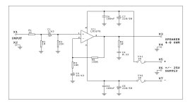
Since my earlier answer you've posted the schematic so I can see how to answer a couple more of your questions.
Firstly about there being two high pass filters - they are rather different. The first one (the input HP) is a true HP and its to protect the chipamp against DC on its input terminal. The feedback HP is not a true HP in that below a certain frequency the response no longer keeps falling. In the technical parlance we say there's a lower frequency pole which cancels out the zero and leads to a flat response. Its because of this flat response at lower frequencies that we also need the input HP.
The answer to question 5 is no.
The remaining questions don't seem interesting enough for me to answer them, perhaps others will chip in. No.6 isn't a question at all. No.7 contains a false premise - there's no need to do impedance matching at audio frequencies.
I'll take a shot at this. As stated, there's no need for impedance matching, and this isn't meant to be an "L pad" anyway. The dB loss is low enough to be insignificant.7.R1(1K) with R2(1M) forms the asymmetric L-Pad atteunator as well as impedance matcher.How we will determine the actual atteunation performed by these two resistors in decibel(db)? and, with what direction (higher side/or lower impedance side) the impedance is matched with these two resistors in k50 diagram?
I want to know the way if and how i could change these values for a different configuration but with the same effect?
We can calculate the loss. Firstly, at audio frequencies C1 is effectively a short circuit (look up the formula for capacitive reactance, and calculate it for this cap at 20Hz and 20kHz), so the bottom side of this "L pad" is actually R2 in parallel with R3. Since R3 is so much lower than R2 (1/10th its value), the effective value is only slightly lower than the lower value, or the value of R3. With R1 this forms a voltage divider of R3/(R1+R3), or 22/23, or just slightly less than 1. Using the voltage-ratio-to-dB formula (I'm too lazy to go through it, but it's not too complicated) it would probably come out in the ballpark of 0.1dB, or (for the purpose of figuring out the gain of this circuit) practically no loss.
But of course that's not what these resistors are there for. R2 is to bleed off any charge on C1 and on any output capacitor of the unit that's driving this amp. R3 provides a DC bias/ground path for the chipamp's input so the output is at (or very near) 0V with no signal. Not sure what the designer was thinking with putting R1 in, though it may offer some protection for an excessively high input signal voltage. Perhaps the chipamp data sheet says something about this.
I think this is a case where "a little knowledge is dangerous." You seem to know a little bit about electronics, but there are big gaps in your knowledge. Get some old textbooks on DC circuits, and then on "AC circuits analysis," plow through them and then you'll know how to do the calculations I described. Doing approximations and knowing when to ignore things (such as R2 for the input loss calculation) is more a matter of feel and experience, of seeing the resistor ratios and doing a gross in-head calculation that tells you "these resistors give insignificant signal loss, so chances are they're there for other reasons," or even "I've seen this type of circuit before with opamps, so I see C1 isolates DC, R3 biases the + input to 0V,..." Then for some of the other questions there are textbooks on the basics of opamps. Don't get the latest current editions used in college electrical courses unless you're actually taking the course - older editions of used textbooks will do fine and are available for much cheaper, virtually for free. There are even websites that teach this stuff.
1) Build and measure it or use a SPICE modeling program.
3) R4/C3 sets the low frequency rolloff and reduces DC offset at the output because it reduces the gain to 1 (from pin 1 of the IC) at DC. C1 prevents DC on the input from getting to the to the speaker. In general the network with the highest corner frequency sets the low frequency rolloff.
4) A small capacitor in parallel with R2 can set the upper frequency rolloff. Otherwise the gain and GBW product with determine the HF rolloff.
5) No
6) R3 and R5 set the closed loop gain by the formula Av=1+(R3/R5). These should be chosen so as the capacitance at pin 2 of the chip and any parasitic capacitance of the PCB do not adversely affect the frequency response.
7) The general formula to convert a voltage ratio to dB is Av(dB)=20*LOG10(V/V). R2 is intended to prevent thumps through the speaker if the source is connected while the amp is powered on. It can be used as a voltage divider if desired. Remember R2 is basically in parallel with R3 for AC frequencies. R1 provides some protection against bad inputs, static discharge and Radio interference.
Recommended literature
Here's my favourite book on understanding opamps - its out of print by the looks of it but there are a few used copies going - bag one while they're still available -
Amazon.com: Used and New: Intuitive IC OP amps (National's semiconductor technology series)
Here's my favourite book on understanding opamps - its out of print by the looks of it but there are a few used copies going - bag one while they're still available -
Amazon.com: Used and New: Intuitive IC OP amps (National's semiconductor technology series)
- Status
- This old topic is closed. If you want to reopen this topic, contact a moderator using the "Report Post" button.
- Home
- Amplifiers
- Chip Amps
- Hi! Please help me with certain issues in LM1875 chipamp design!