In the datasheet of the LM3886 you find:
- a schematic of a typical application (fig. 1) with no (extra) feedback compensation network and
- a test circuit # 2 and a typical application (fig. 2) with a feedback compensation network consisting of a Cc (220 pF), a resistor Rf2 (20 k) in serie with Cf (50 pF).
In many applications, especially the do-it-yourself kits, you find no feedback compensation network, but in some schematics you will find them, sometimes only the Cc of 220 pf and sometimes this Cc together with Rf2 and Cf.
I'am interested in the influence of these extra compensation components.
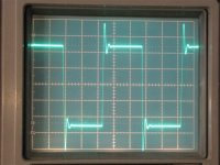
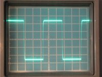
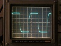
So I put a block signal of 20 kHz on the input of the amplifier (no input filter). This is what I saw on my scoop:
The first smooth image is without any compensation components. The second with the overshoot is with only the Cc of 220 pF. And the last image with the oscilations on the sides is with Cc, Rf2 and Cf.
I call for comments. So far I am sure: I will not use the (extra) compensation components, although National Semiconductor suggests with reserves to do so.
Marc.
- a schematic of a typical application (fig. 1) with no (extra) feedback compensation network and
- a test circuit # 2 and a typical application (fig. 2) with a feedback compensation network consisting of a Cc (220 pF), a resistor Rf2 (20 k) in serie with Cf (50 pF).
In many applications, especially the do-it-yourself kits, you find no feedback compensation network, but in some schematics you will find them, sometimes only the Cc of 220 pf and sometimes this Cc together with Rf2 and Cf.
I'am interested in the influence of these extra compensation components.
So I put a block signal of 20 kHz on the input of the amplifier (no input filter). This is what I saw on my scoop:
The first smooth image is without any compensation components. The second with the overshoot is with only the Cc of 220 pF. And the last image with the oscilations on the sides is with Cc, Rf2 and Cf.
I call for comments. So far I am sure: I will not use the (extra) compensation components, although National Semiconductor suggests with reserves to do so.
Marc.
Attachments


I recommend all the "optional" components. RF attenuation, Zobel R+C, Output inductor L//R,
Cs must be fitted very close to the power pins. The leads between the two sets of Cs must be very short.
I do not recommend that Cc (200pF) be directly connected to -IN. -IN is very susceptible to capacitance causing instability. Mount the two feedback resistors very close to -IN. Connect Cc to the other side of the lower leg NFB resistor. This is the ground end of Ri+Ci.
Try increasing the gain to see the effect on the overshoot. That middle plot showing significant overshoot looks typical of a PM<60° and probably much lower.
With the right combination of components and lead lengths and gain the overshoot should just about disappear before the square wave becomes too "rounded". This is a good clue to PM of 80°
I would not use Cf + Rf2, until I had a lot more experience on stability compensation. I don't believe adjusting those two component values are a beginner task. However in discrete amps Cf~3pF to 10pF are often used to trim in the stability.
Last edited:
I already use a Zobel R+C, an output inductor L//R: see schematic.
I also use Cs's fitted very close to the power pins.
My question was if it is better or not to apply the feedback compensation network as suggested in the datasheet. So I did the experiment with and without those components and I found it is (much) better not to use them.
You confirmed my results. Indeed connecting the Cc of 220 pF to the -IN causes overshoot and makes the amplifier more sensitive for oscillation. You better connect it to the ground, making it an input filter. I apply an input filter of 1 Kohm + 1 nF, so the - 3 dB point will be app. 160 kHz.
You also confirmed not to use Cf + Rf2.
I think the LM3886 is a good product. I am suprised why they give in the datasheet the wrong advises.
Marc.
Attachments
Could you post the scope shots of the 3886 output with the components in the new locations.
This way others can see directly the before and after.
How long, in millimetres, are the lead lengths of the Cs capacitors? (8 leads for the 4 caps).
How long are the route lengths of the Cs capacitors? (4 routes from cap body all the way around the loop back to the cap body).
This way others can see directly the before and after.
How long, in millimetres, are the lead lengths of the Cs capacitors? (8 leads for the 4 caps).
How long are the route lengths of the Cs capacitors? (4 routes from cap body all the way around the loop back to the cap body).
Last edited:
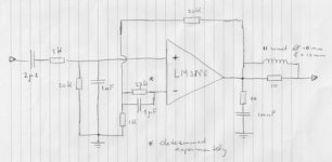
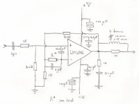
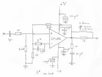
Hereby the schematics and the corresponding scoop shots of the output.
As you see the basis version gives a clear square wave, the version with the Cc of 220 pf gives overschoot and the version with the Cc, the Rf2 of 20 k and the Cf of 47 pF gives oscillations on the sides.
The value of R* is determined experimentely to cancel the offset voltage on the output. For one amplifier the value is 27k for the other 18 k. This gives an output offset of around 1 mV. This offset voltage hardly drifts (less than 1 mV) when the amplifier gets hot. The R*//C of 1 microF does not influence the scoop shots of the output.
The lead lengths of the Cs capacitors are 5 mm to the + or - and from there 20 mm over the PCB to the LM3886 connections. The lengths of the other sides to the ground on the PCB are 10 - 20 mm.
Maybe you know the answer why National Semiconductor suggests tot apply Cc, Rf2 and Cf?
Marc.
Attachments

If that second scope shot is typical of what other builders get in their builds then I will surmise and state "no wonder they all hear changes in sound quality when they swap in and out other components.
First one must get the amplifier working properly.
Then one can look for "improvements".
First one must get the amplifier working properly.
Then one can look for "improvements".
When I add a C of 220 pF from the + input to the ground in the basic version (the schematic most on the left), I see a very very minimal difference in the way that the bends rounds a little bit more on the tops. But the difference is too small to recognize it on a shot.
The difference is of course greater when you increase the value of the capacitor. Then you see more sooth bends with no oscillations or what so ever. What you is is a normal R-C filter.
I think I am going to use a capacitor from + to ground with a value of 1000 pf (- 3 dB point = 160 kHz) or 1200 pf ( - 3 dB point = 132 kHz). The phase shift at 20 kHZ is then less than 10 degrees. I sometimes hear that a phase shift of less than 10 degrees is not audible, but more dan 10 degres may be audible.
Marc.
Thanks for confirming that the "normal" location of RF attenuation Capacitor does not show a marked change in the stability response of the 3886.
Could you now show what happens in pic 3 with the RF moved to the normal location?
It seems that you are confirming what many have found:
The National datasheet was cobbled together without proper consideration for the skills of those who were about to read and implement.
Or more simply:
The 3886 datasheet is riddled with mistakes!
btw, those are my interpretations.
Hallo Andrew,
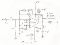
Hereby the picture with Cc (220 pF) from + input to ground and with Cf (47 pF) in serie with Rf2 (22 k) from the output to the - input.
When I disconnect Cc, there is hardly no difference.
As you thought, the oscillations are caused by a Cc between the + and the - input!!
The conclusion must be: never use a RF attenuation capacitor between the + and - input but always - in the non-inverting situation - between the + input and ground.
Can you tell me what is best to do:
- Only a capacitor Cc between + input and ground to make a low pass filter or;
- A capacitor Cf in serie with a resistor Rf2 from the output to the - input or
- A combination of those two?
What will then be the best values?
Marc.
Attachments
It's the same in an inverting amplifier arrangement. Never hang the RF attenuating cap directly off the -IN pin.
Always split the input resistor and run the RF cap from between the two input resistors.
So, I ask the question again:
How many builders are using 3886 with the RF cap directly on the -IN pin and as a result listening to a misbehaving amplifier?
Always split the input resistor and run the RF cap from between the two input resistors.
So, I ask the question again:
How many builders are using 3886 with the RF cap directly on the -IN pin and as a result listening to a misbehaving amplifier?
I have no answer on your question. It is the first time that I apply the LM3886.
Maybe we should warn all the LM3886 users?
What I don't understand is why this is a conversation only between you and me about an essential issue in the practice of the LM3886?
So I call for all the users of the LM3886 to reply on the issue of the RF capacitor of 220 pF between the + and - input, as stated in the datasheet. What are your experiences and what happens with the sound (at high level) if you disconnect this capacitor?
Marc.
This thread made me quite curious, so I made a measurement. The Loop gain of the LM3886 I tested (+/-36 volt supply), configured for a gain of 21, crossed over to unity at 348 kHz. The phase margin was 78 degrees. That's perfectly fine. (The measurement was made with an 8 Ohm load, but didn't change much with level, or when adding 0.1 uF across the 8 Ohm load).
The feedback network was just a 20K feedback resistor and a 1K resistor from inverting input to ground. There were no extra caps...no 220 pF...no add'l RC's as shown in the data sheet.
It would seem that at that gain, that's about all you'd need. Now I've made and sold a number of these configured according to the National recommendations, and they sound fine and are quite stable. I have also seen the square-wave funnies that Marc Vi noted with National's standard compensation.
I'm guessing that it's not audible because nothing in real program material ever excites that little bit of funny business. However, I'm quite inclined to seriously investigate removing three components, C4, C9, and R12 as shown in this schematic:
http://www.updatemydynaco.com/documents/AmplifierModuleSchematic_2011_10.pdf
With the RF filter (R4/C3) on the front end, I don't think that RF on the input should be an issue. Maybe C4 helps a bit for RF pickup on the speaker wires. Perhaps National went that way based on someone who was close to a broadcast transmitter.
So, my curiousity about the seemingly worthwhile simplification is tempered by a bit of caution, but it certainly seems like a worthy investigation.
Dan
www.updatemydynaco.com
Last edited:
I should have asked at the time, silly me........... The Loop gain of the LM3886 I tested (+/-36 volt supply), configured for a gain of 21, crossed over to unity at 348 kHz. The phase margin was 78 degrees..............
How would he have measured the unity gain frequency and the phase margin?
What I don't understand is why this is a conversation only between you and me about an essential issue in the practice of the LM3886?
...why National Semiconductor suggests to apply Cc, Rf2 and Cf?
Can you tell me what is best to do
The 3886 datasheet is riddled with mistakes!
<< why this is a conversation only between you and me about an essential issue in the practice of the LM3886? >>
My guess: everybody was so stunned by your research that they were speechless. Especially since you tested with square waves, which are death come a-calling to amplifiers.
Many self-proclaimed experts deride the data sheet's Typical Application circuit. They change the circuit to add complexity, add components to increase cost, and then, having made an easy job difficult, announce that now everything is better.
But none of these experts are known to be working in the R&D departments of international corporations, and your tests seem to indicate why. So I'd say that being struck dumb is the correct response.
<< ...why National Semiconductor suggests to apply Cc, Rf2 and Cf? >>
They don't. The same data sheet warns that these and other optional components have "specific desired functions," and that "... they may cause certain undesirable effects when they interact." It goes on to urge, "Please take careful note of basic amplifier component functionality when designing in these components."
These chips are used by many different customers in many different ways. The optional components are the factory engineers' advice to customers that this-or-that additional component should be used when that-or-this special function is needed. The engineers are saying to customers, "You don't need to re-invent the wheel, we already did the work for you, here it is." None of it has anything to do with building a straightforward, single purpose audio amplifier--as is shown by your tests.
<< Can you tell me what is best to do >>
Tell you what to do? You gotta be kidding. People should be asking you what to do.
This thread is more than two years old (I ran across it by chance), but your research is as valid today as it was then. A vote of thanks, at least from me, for publishing this valuable information.
<< The 3886 datasheet is riddled with mistakes! >>
This statement appears to contradict the very test results you're looking at, which are Marc Vi's scope traces.
I think it's worth considering that it costs tens of thousands of dollars to create an op amp--or not unlikely hundreds of thousands. Teams of at least one senior, and several junior, engineers work on such a project using very expensive test equipment. Everybody on the project can be expected to have at least a master's degree, while nobody graduated in the bottom ten percent.
But the design expense is small compared to the cost of building a factory full of automatic machines, which is the only way op amps can be manufactured. Building such a factory costs not thousands of dollars, but millions.
Then after all of this expense, would anybody let the success of their chip depend on some half-written, slapdash document full of errors?
I know I wouldn't. I'd have the data sheet checked by every engineer on the development team, proofread in another department, checked again, this time by consulting engineers, proofread again, and this would continue until everybody voted "no errors." I can't imagine that anybody would do anything different.
All of which is borne out by Marc Vi's research. The Typical Application circuit gave him near-perfect square waves, while the optional components--those intended only for special functions--did not, just as the factory warned. It would seem that the proof is in the scope trace.
.
Last edited:
A blast from the past here...seeing this thread again...
So after a few more years of experience with LM3886...why the funny cap across the inputs (inv to non-inv) and the extra RC in the feedback?
The answer is...when you drive the amp hard enough and it's hot enough that the Spike protection starts to limit output power, those extra components delay the onset of, and diminish the amount of HF oscillation caused by the Spike circuit.
If you're using the part quite conservatively, I don't think you'd need that stuff...but if you're selling it in numbers where by definition some fraction of users will be beating on it hard...these components civilize the behavior with no real side effects except the visual...
...why the funny cap across the inputs (inv to non-inv) and the extra RC in the feedback?
The answer is...when you drive the amp hard enough and it's hot enough that the Spike protection starts to limit output power, those extra components delay the onset of, and diminish the amount of HF oscillation caused by the Spike circuit.
Ah, then you'd employ the optional components toward achieving a specific desired function. Making an informed decision to accept certain undesirable effects because they were not significant to your purpose. Hmmm, well yes, I see.
.
Here are my $0.02 worth:
First off, let's make sure you have a clean setup. I suggest removing R* and C* (the two components for the input bias current compensation). Secondly, make sure that your function generator is terminated properly. If your function generator has a 50 ohm output, use a 50 ohm coax cable to connect to the amplifier, and ensure that the input impedance of the amp is 50 ohm. You can do this by either soldering 50 ohm (49.9, 51, or two 100 ohm in parallel will work) from the input connector center pin to ground. There are also these handy-dandy feed-thru terminators for this exact purpose. HP/Agilent/Keysight 10100C, for example. This ensures good fidelity on the incoming square wave.
Strip off all the "optional stability components" (Rf2, Cf, Cc). Load the amp with an 8 ohm power resistor. Now run a sine wave into the amp. Crank up the amplitude until the amp starts to clip. You will notice a spurious oscillation near the peaks of the sine wave. I'm guessing it's a saturation clamp inside the LM3886 that oscillates. That's mentioned in the data sheet. National used the term "quasi-oscillation".
Now start adding Cc. You'll find that you get the cleanest clipping response with Cc in the range of 150 pF to 220 pF. I've settled on 180 pF. This may depend slightly on the PCB layout, decoupling networks, and such.
Cc performs noise gain compensation on the amplifier. If you now examine the transient response (so square wave in, 10 kHz, say 20 Vpp on the output of the LM3886 on +/-28 V rails), you'll notice a hump on the flat parts of the square wave by the edges. In other words, the amp now has a bit of overshoot due to the capacitive coupling through Cc. To deal with this and get a clean transient response, add Rf2 and Cf. You'll find that the 20k+47 pF (or 50 pF) mentioned in the data sheet provides good performance (assuming a closed loop gain of +21). If you use different feedback impedances than the 1 kohm, 20 kohm mentioned in the data sheet, you need to scale Rf2 and Cf accordingly. Be careful, though... I suggest looking at the loop stability in a circuit simulator before trying it out in the lab.
Now set up the same circuit in your favorite circuit simulator. Include the parasitics associated with the various components and the layout on the feedback impedances. As a rule of thumb, use 10 nH in series with all passive components and a 2 pF cap from end-to-end on resistors (so Zresistor = (R + L)||C, where R is the resistance marked on the resistor, C is 2 pF, L is 10 nH. This might be a tad conservative on the C (I measured some metal film resistors, they measure 100 fF end-to-end) but the layout can add quite a bit, so it's probably OK.
Now, simulate the loop gain. You'll notice the parasitics, in particular those across Rf, create a pole-zero pair in the 1-10 MHz frequency range. Add the Zobel network (C+R to ground). That cancels this pole-zero pair. The values provided by National - 2.7 ohm, 100 nF are close to optimal.
Add some load capacitance and watch the phase margin go to crap. That's what the Thiele network (L || R in series with the output) is to combat. 1-2 uH is about right. Higher is better, but too high reduces the dampening factor at 20 kHz. With the Thiele inductor in place and a reasonable load cap (say 100 nF) you'll notice the amp rings like you wouldn't believe. The resistor in the Thiele network dampens that out. I suggest aiming for a Q of about 1 for a load cap of 1 uF. You'll end up with R = 1.5 ohm.
2 uH is 15 turns wound on an AA size battery. (Thanks to AndrewT for the idea of using an AA battery as a coil former).
~Tom
Last edited:
Then after all of this expense, would anybody let the success of their chip depend on some half-written, slapdash document full of errors?
I know I wouldn't. I'd have the data sheet checked by every engineer on the development team, proofread in another department, checked again, this time by consulting engineers, proofread again, and this would continue until everybody voted "no errors." I can't imagine that anybody would do anything different.
Try reading the TDA7293 sheet.
") It's got some good information, but does leave you wanting for more. The LM3886's datasheet is very thorough, although I'd love to know if modern semiconductor processes have changed anything about a "minimum" device (higher UGBW?). It seems a fair number LM3886 of circuits lately have been run at ostensible phase margins that have them oscillating.
It's got some good information, but does leave you wanting for more. The LM3886's datasheet is very thorough, although I'd love to know if modern semiconductor processes have changed anything about a "minimum" device (higher UGBW?). It seems a fair number LM3886 of circuits lately have been run at ostensible phase margins that have them oscillating.- Status
- This old topic is closed. If you want to reopen this topic, contact a moderator using the "Report Post" button.
- Home
- Amplifiers
- Chip Amps
- LM3886: the effect of the compensation network Cc, Rf2 and Cf