Hi all,
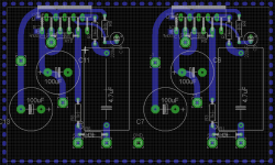
I'd like to put together a good PCB for the LM3886 (that is bridgeable for mono output). I don't have much Eagle experience, however I have found an existing PCB design on the 'net. I have attached it and the schematic to this post. First off, could anyone think that this board is missing any feautres that could be added easily? Are components meant to be soldered directly to the chip?
Thanks and regards,
Chris
Attachments
The LM3886 data sheet can be found here: http://www.ti.com/lit/ds/symlink/lm3886.pdf and is recommended reading for anyone using the chip.
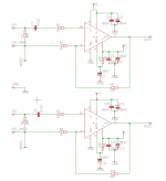
The muting circuit would be made by installing a switch between the negative rail and pin #8. National's data sheet shows it between V- and Rm (your 27kR resistor), but I suppose it could go anywhere between V- and pin #8. Presumably, you would have wires coming off the board, to a switch mounted on your chassis. Open the switch to mute the amplifier. It's entirely optional.
The Zobel network is a very general term for a variety of filters. National's LM3886 data sheet shows a low-pass zobel network consisting of a 0.7uH inductor and a 10R resistor in parallel, between pin 3 and the 8R speaker load, but only in their single supply application circuit (fig 2), not in their "typical application" (fig 1). I don't know why that is. A popular commercial design puts a 2.7R, 2W resistor and a 0.1uF nonpolar cap in series, parallel to the speaker load. It will just filter out some high frequency noise. I can't predict whether or not it will improve the sound of the amp.
All amplifiers IMHO, should have fast-blo fuses just downstream of the power supply - on both rails. Once, my fuses saved me a lot of repair work when a screw fell into the amp, and wedged its self in between the PCB and the heatsink. I didn't know it was there, and when I turned on my amp, both positive and negative rail fuses blew! Something like this http://www.littelfuse.com/data/en/Data_Sheets/656_659_660_LF_060102.pdf would be perfect.
The muting circuit would be made by installing a switch between the negative rail and pin #8. National's data sheet shows it between V- and Rm (your 27kR resistor), but I suppose it could go anywhere between V- and pin #8. Presumably, you would have wires coming off the board, to a switch mounted on your chassis. Open the switch to mute the amplifier. It's entirely optional.
The Zobel network is a very general term for a variety of filters. National's LM3886 data sheet shows a low-pass zobel network consisting of a 0.7uH inductor and a 10R resistor in parallel, between pin 3 and the 8R speaker load, but only in their single supply application circuit (fig 2), not in their "typical application" (fig 1). I don't know why that is. A popular commercial design puts a 2.7R, 2W resistor and a 0.1uF nonpolar cap in series, parallel to the speaker load. It will just filter out some high frequency noise. I can't predict whether or not it will improve the sound of the amp.
All amplifiers IMHO, should have fast-blo fuses just downstream of the power supply - on both rails. Once, my fuses saved me a lot of repair work when a screw fell into the amp, and wedged its self in between the PCB and the heatsink. I didn't know it was there, and when I turned on my amp, both positive and negative rail fuses blew!
Something like this http://www.littelfuse.com/data/en/Data_Sheets/656_659_660_LF_060102.pdf would be perfect.The parallel L+R is commonly known here as "the output coil". It's function is to damp oscillation when the amp drives capacitive loads and becomes unstable (rings). It's a safety measure and it also forms a LP filter than gently attenuates anything above the rolloff point. It can be placed anywhere inside the case....... National's LM3886 data sheet shows a low-pass zobel network consisting of a 0.7uH inductor and a 10R resistor in parallel, between pin 3 and the 8R speaker load, but only in their single supply application circuit (fig 2), not in their "typical application" (fig 1). I don't know why that is. A popular commercial design puts a 2.7R, 2W resistor and a 0.1uF nonpolar cap in series, parallel to the speaker load.....
The Zobel is the series R+C part that acts as a snubber for HF switching spikes and low level oscillation in the output stage. It needs to be as close as possible to the chip output pins to be effective. Use good, low inductance parts.
The values for these networks are a case of "one size fits all" for class AB amps.
Last edited:
And the Zobel network, and the output coil and its parallel resistor, all together, are called the Boucherot network, if I recall correctly.
They are usually thought of as stability compensation networks, rather than as filters, although the coil and resistor do help to filter RF that would otherwise more-easily enter through the output, which can be a major problem as far as RF-avoidance is concerned.
A Boucherot network should always be used on power amplifier outputs, in my opinion.
Note that the output inductoir should be an "air core" type coil. It should not be wrapped around the resistor, for example. Yes, I realize that you will have seen it done that way, very often. But it's not the best way to do it. Unless it's a true air core coil, there will be some potential for hysteresis distortion. (And, of course, if it's got a ferrite or ferric metal core like iron or steel, then there would also be a potential for core saturation.)
There is a nice air-core inductor calculator, here: Pronine Electronics Design - Multilayer Air Core Inductor Calculator
There are also single-layer ones available (Google for air core coil calculator).
For the PCB:
Is the ground layer missing from the image?
The 1000 uF caps need to be connected as close to the power pins as possible, to avoid as much trace inductance as possible. Otherwise, transient response will be less optimal and power rail disturbances will be larger. Also, the trace-lengths for V+ and V-, from the caps to the chip pins, should be closer to being equal.
The caps for the negative rails should be way up next to the chips and rotated around their + terminals by 135 degrees or so, clockwise. And the ones for the positive rails should be rotated around their + terminals, clockwise, by 90 to 135 degrees and moved up as close to the V+ pins as possible.
The V- inputs should be on the other side of the cap, i.e. upstream from the cap with respect to the chip.
The input signal sections should have a separate signal-ground plane area, to avoid the creation of enclosed loop area between signal input and signal input ground. Alternatively, the signal input and signal input ground paths must be re-routed so that there is a minimum-possible gap between them, everywhere. Otherwise, they can and will have time-varying currents induced in them by any time-varying magnetic fields, including AC Mains and maybe also RF. (The existing power ground plane will have very little shielding effectiveness against local magnetic fields so the signal and signal ground conductors still need to have as little as possible enclosed loop area between them, to prevent them from being a hum antenna.)
In case the main ground layer does also include the input signal grounds, those should be kept completely separate and should be able to go back to the star ground at the power supply separately. (It looks like they might already have separate connections but I can't be sure without seeing the ground layer.)
The input capacitor used could be a different size or type, with different lead-spacing requirements. In order to also help eliminate the enclosed loop area between signal and signal ground, extend copper from one capacitor pad almost all the way to the other pad, and also almost all the way over to the signal ground trace, and as close to the chip pins and input pads as possible. Additional capacitor mounting pads can then be added, for various lead-spacings.
What is connecting the input terminals? If it is a resistor then I believe it has to be AFTER the input capacitor. If it's a cap then it should be at the chip's input pins.
Basically, all components should connect as close to the chip pins as possible, to avoid having stray inductances or capacitances (or RF antennas) connected to the pins.
Why is there a resistor in series with the Vin- trace?!
There should also be pads in place for input RF low-pass RC filters, just before the chips' input pins. Alternatively, a 220 pF capacitor directly across the input pins would work.
Last edited:
- Status
- This old topic is closed. If you want to reopen this topic, contact a moderator using the "Report Post" button.
- Home
- Amplifiers
- Chip Amps
- LM3886 PCB Layout