The design is improved from the first drawing but he charging currents and the feedback and output currents still don't seem to be sperated completely.
I thought that it was normal to use a diamond configration to the capacitors and put the start point on the output side of the diamond . The bulk capacitors should form the referance point, not the return to the bridge.
So ground comes from the connector, seperates to the two caps then comes back together again after the caps. Where it comes back together is the start point. (forming a diamond shape) This completely seperates the charging current for the caps from the signal currents which are then returned to the star.
Regards,
Andrew
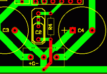
You are half way there. Repeat the same shap on the otherside of the caps and attach all the other returns to that point rather than your connector and you have seperated the input charging currents from the feedback and output currents. You shoudl then have a box on its side type shape the diamond I was talking about earlier.
So the only connection to the connector should be the two traces going to the caps. All the other connections shoudl be on the other side of the caps on the output traces from the caps.
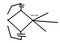
Please see 5 year olds drawing of this arrangement") sorry it is so rough.
sorry it is so rough.
So the only connection to the connector should be the two traces going to the caps. All the other connections shoudl be on the other side of the caps on the output traces from the caps.
Please see 5 year olds drawing of this arrangement
sorry it is so rough.Attachments
Without seeing the rest, I don't know, but note that the ripple from the caps running alternately through the little green track in the middle bottom part will generate a ripple voltage that, through R4/C2, will be input to the amp.
What you need to do is take a decision: chose a point and declare that your star ground. Now, route everything to it without common tracks. It's really that simple.
Jan Didden
What you need to do is take a decision: chose a point and declare that your star ground. Now, route everything to it without common tracks. It's really that simple.
Jan Didden
Hi Jan,
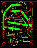
thanks very much for willing to comment (and apologies to Supereri - hope you may benefit of my intrusion in your thread). My original idea was like that:
http://www.diyaudio.com/forums/showthread.php?postid=222827#post222827
mutuated from the original circuit description and picture by Thorsten Loesch, from which Supereri #1 Pcb was derived. Is this the best grounding approach, or there is something to improve?
Thank very much in advance for your answer. It would also be very happy if you could suggest me a tutorial or some readings on this topic.
Ciao,
Massimo
Massimo,
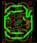
I think your referenced PCB is as good as they come, tracking wise. But, since you ask, let me tell you what I would change, although the effect would probably not be audible.
- What is the purpose of C2? Don't you want to use 2 C2-s, one each across C3 and C4?
- There is a hole to the left of R5, is this used?
- I would clean up the PCB a bit, for instance center the hole on the C3 left pin etc.
- Looking at the tracking, for instance the track from C4 underneath R2, I would have put C4 on the left and C3 on the right. That would make it more compact and the tracks shorter.
Anyway, I really AM nitpicking here, and the PCB as it is excellent for a GC IMHO.
Question: If memory serves me well, don't you want to use a zobel at the output? I didn't see it at the PCB.
Jan Didden
Chapeau!
Jan,
Thanks once again for your great advice!
Ciao,
Massimo
P.S. Humblest apologies to Eric for hijacking Jan Didden. I candidate myself to the Sin Bin.
Jan,
thanks very very much for your help, comments and kind words. My background is not in electronics, so I really have a lot to learn.But, since you ask, let me tell you what I would change, although the effect would probably not be audible.
Many of the oddities of my pcb deal with the idea of allowing alternative components to be used by the fellow audiodiyers. This is the case of C1, C2 and C4. I also added one more pad to allow a "longer" R5. As far as I understand Thorsten's schematics, R4 should be for minimizing DC offset and C2 to short AC to ground (did I answer your question? Maybe not...). Btw, the latest version, in the same thread, is even more crowded of options, but having included the ExpressPcb files, anyone can remove whatever is not needed.- What is the purpose of C2? Don't you want to use 2 C2-s, one each across C3 and C4?
- There is a hole to the left of R5, is this used?
Ehm... this was to make more evident the square pad, to help the inattentive people like me to solder C3 the right way.- I would clean up the PCB a bit, for instance center the hole on the C3 left pin etc.
Thanks very much for the idea. Tomorrow I'll try to exchange the caps.- Looking at the tracking, for instance the track from C4 underneath R2, I would have put C4 on the left and C3 on the right. That would make it more compact and the tracks shorter.
Thorsten's circuit uses a .22 Ohm res, while the datasheet uses 10 Ohm paralleled with .7uH. The latest version of Pcb (in the thread) should allow both.Question: If memory serves me well, don't you want to use a zobel at the output? I didn't see it at the PCB.
Thanks once again for your great advice!
Ciao,
Massimo
P.S. Humblest apologies to Eric for hijacking Jan Didden. I candidate myself to the Sin Bin.
Could someone spotcheck this one
Hi all,
When I built my GC there were only a few folks who were using boards and Scott Nixon's were not quite finished up yet, so I embarked on designing these, never having done it before. I have been using this amp for quite a while now with no problems and great sound. Now that I have found this thread, after a long time away from building GCs, I should have those of you with much more knowledge on this topic than I look over my design. I tried to set things up to use different sized, and multiple caps (I had a bunch of Nichicon 470ufs laying around, hench the dual PS caps) and it can be configured as inverting or non. I'm running in the non-inverting mode and it's quiet and stable...more than I could say for most of my dead-bug attempts!
Thanks for any input anyone might have,
Tom
Attachments
I probably should add that I use the leads from the resistors/cap to jumper to the ground buss. I also did not add the zobel or a .22ohm on the output, and left out the input cap on the non-inverted version. I figured that if these were needed, they could be done off the board. My current amp seems to be doing fine without any of these. Also, I connect the speaker "-" to the first large hole, and the PS CT to the second, leaving the small signal grounds on the opposite side of the PS CT point. Those small holes in the ground buss are used to pull the jumpers or component leads through and solder them in place. Quirky, huh?
Tom
Tom
another version
Hi antomas,
Thanks for you input. I did a little rearranging and here's what I have come up with. I'm trying to set it up so it can still be built as inverted or non and that has proven to be the hardest part. The resistor sizes are purposely large to accomodate .5W Rikens. From a grounding standpoint, I thik this is better than my previous boards. I was able to squeeze in the .22 on the output but had to drop one of the small value caps from the power rails. I remember that many folks were using a 1uF between the + and - rails, so I do have the option to add that cap.
Any other pointers.
Tom
Attachments
- Status
- This old topic is closed. If you want to reopen this topic, contact a moderator using the "Report Post" button.
- Home
- Amplifiers
- Chip Amps
- PCB Layout check