Planning to get some PCBs fabricated for the LM3886 amplifier based on special audio application circuit.
Any comments on fine tuning are most welcome.
Any comments on fine tuning are most welcome.
An externally hosted image should be here but it was not working when we last tested it.
Attachments
A minor alteration. Mute cap moved to one end.
An externally hosted image should be here but it was not working when we last tested it.
Attachments
C5 is too far away from PIN4.
The copper trace to PIN5 is too thin.
Try to squeeze all the input components into a much smaller area with much lower Loop Areas.
Allow multi PIN Pitch for all capacitors.
You have two Power Ground Terminals on the PCB.
They both cannot be connected to Main Audio Ground (MAG).Which do you plan to use?
Connect1 must not be used to jumper power to PIN1&3
The tapping for power to PIN1&3 must come from the decoupling cap PIN.
Last edited:
Thankyou Mr.Andrew for your valuable comments. I am able to further finetune the PCB.
The 2 power ground terminals are for supply_ground and audio_out ground.
For V+ supply i'll use a jumper_wire of 1.5mm gauge.
The 2 power ground terminals are for supply_ground and audio_out ground.
For V+ supply i'll use a jumper_wire of 1.5mm gauge.
An externally hosted image should be here but it was not working when we last tested it.
Concur with AndrewT, including that the copper pour for pin 1 should be smaller on the left side so that the ground island can protrude into that area (almost to pin 1). You should then be able to move the connector and get the C5 decoupling/bypass cap connected to the ground pour from pin 4 directly, or from pin2.
You can change the shape of the pads for the chipamp so that they are larger toward the front and rear of the chip but smaller on the side that is toward the middle of the rows of pins. That way, you can use larger traces when going between the rows. If you can't make the pads that way with the software you're using, then just use a much smaller pad style and make up the difference with the traces and pours that connect to them.
Ideally, you would want to have the V+ and V- paths be symmetrical and as identical in length (to power pins) and width as possible.
If you are going to jumper the power that way, or even if you weren't, then each power input's copper area needs to narrow down to the size of the 1000 uF caps' pads and then can widen out again on the downstream side, which is where the jumper connectors (and everything else) would have to be connected.
Also, the output ground (and Zobel network ground) should have the same distance to (and be close to) each of the 1000 uF caps' ground pins. So they should be rotated to the left to be between the caps' gnd pins (if you were going to keep the rest of the layout the same).
Resistors (and all other components) that connect to any chipamp pins, especially the input pins (and power and output pins), should be connected as close as possible to the pins.
The components that connect to the output pin all need to connect closer to the pin.
Input signal and input signal ground traces should stay absolutely as close together as possible, at all times! They don't need to follow the component alignment. They must follow each other. Every little bit of area between them makes them into a better hum antenna and a better RF antenna.
Also, I would want the audio input reference ground to return to the PSU separately, at least as an option, rather than connecting to the dirty power ground through the 2 Ohm R2.
All acute angles (less than 90 degrees) should be changed to be 90 deg or more.
Are you certain that you can't make a double-sided PCB? If you can't (or either way, actually), you should consider mounting some of the components on the bottom of the board, and/or directly to the chip pins (e.g. the small decoupling/bypass caps, the 200/220 pF RF filter on the input pins, the feedback network components).
If soldering directly to a chip pin, make sure that pin is heatsinked BETWEEN the chip and where you will solder! For example, you could use a rubber band around the handles of long-nose pliers to clamp the tip of the pliers to the pin, before soldering.
Edit: You posted a new layout while I was typing. But I think that most of my suggestions still apply.
Edit 2: What is the max current capacity of the inductor you are going to use? (But I do agree that it should not consist of wire wrapped around the 10 Ohm resistor. However, it should be an AIR-core inductor, probably just a hand-wound coil of thick-enough wire. There are on-line inductor calculators for air-core coils, but they usually assume that you have magnet wire. Otherwise, the thickness of the insulation changes the calculations.)
Last edited:
Thanks Mr. Gootee for really giving time and writing all the feedback. Actually i am following some personal guidelines for track routing which i learned over 2-3 years of DIY pcb making.
1. First is that the resistors should not be placed near or on the power IC, i have noticed that during running the IC pins and IC mounting area also gets heated up. So i decided the feedback resistor will be outside the IC and in open ventilated area.
2. I'll do provide the earth pour for signal side area.
3. regarding the zobal i'll try to move it to the other side, so near to power capacitors.
The inductor will be of 1.5mm 15 turns copper wire. OD of 7-8 mm
And i am planning to fabricate the Single side PCB for cost effectiveness, i am also planning for a double layer later after getting a quote from PCB fabricator.
and presently, earthing i am planning on the same PCB, so that i can save on PS design. If i design PS then i'll sure include your signal ground point.
Thanks.
Thanks Mr. Gootee for really giving time and writing all the feedback. Actually i am following some personal guidelines for track routing which i learned over 2-3 years of DIY pcb making.
1. First is that the resistors should not be placed near or on the power IC, i have noticed that during running the IC pins and IC mounting area also gets heated up. So i decided the feedback resistor will be outside the IC and in open ventilated area.
2. I'll do provide the earth pour for signal side area.
3. regarding the zobal i'll try to move it to the other side, so near to power capacitors.
The inductor will be of 1.5mm 15 turns copper wire. OD of 7-8 mm
And i am planning to fabricate the Single side PCB for cost effectiveness, i am also planning for a double layer later after getting a quote from PCB fabricator.
and presently, earthing i am planning on the same PCB, so that i can save on PS design. If i design PS then i'll sure include your signal ground point.
Thanks.
I can see why you have made the choice about the resistors. But let's analyze it in more detail, just for fun:
So the resistors might get too warm if you place them closer to the chip? Maybe so, if you place them against the chip or the heatsink, although even that might not actually hurt them, much. But if that was the only consideration, I would agree, of course. However, there's a trade-space to analyze and you have only mentioned one part of it. In the case of the negative input pin of an opamp or chipamp, a length of undamped conductor there increases the tendency toward instability, due to parasitics. It also increases the tendency for RF pickup and other EM coupling. So connecting the resistor close to the pin is a best practice, for the performance and health of the circuit as a whole. Do you actually know the thermal-related specs of the resistor, and the potential magnitudes of the thermaly-induced problems, for a resistor mounted down on the PCB and connected near the negative input pin of this chipamp? I do not, but would assume that the risk would be negligible. But, not placing it near the pin could cause the much-more-expensive chipamp to overheat, if it oscillated, and it could possibly even be destroyed. Admittedly, both of the risk scenarios (yours and mine) seem somewhat unlikely to occur. But if you have to choose, you always pick the one that has both greater potential benefits and also alleviates the greater risk.
Somewhat similarly, it is well-known that the feedback path should be kept as short as possible, to alleviate the risk of instability and to improve performance. I do not think that the heat will be a big-enough problem, especially if you leave a small gap between the chip and the resistor. But leaving too much space between them, with relatively-long conductor lengths, might cause a lot more heat, if the chip rings or oscillates. Anyway, you could easily add a small heat sink to the resistor, if you really believed it was a big-enough problem. But again, you should also look at the manufacturer's data sheet for your resistors and you might find that they are fine with quite a lot of heat. In the end, I believe that the same risk analysis with the same result will apply for the critical length of the feedback path.
Note, too, that there is possibly some coupling between the things we both mentioned: If you put the resistors close, where they might get hot if the chip gets hot, then the chip might stay cooler and the problem could go away. But if you put them farther away to keep them cool, then the chip might get much hotter than it would have, and the resistors might then still get too hot but you've also got a much bigger problem with the chip itself possibly overheating.
As usual, with trade-offs, you would need to try to first determine the relative magnitudes of the consequences, and their probabilities of occurence, and thus determine the associated risk levels, before you made the final engineering judgment. But usually the main thing is probably knowing what the real trade space dimensions are, to begin with, so you can analyze all of the right risks.
Anyway, those weren't the most-important suggestions, actually.
The most-critical one is probably about the enclosed loop area of the signal input and signal input ground conductors.
The input section is before the amplfication so even small effects, there, can have relatively large effects on the output.
The separate ground conductor for the signal input section's ground reference voltage is also very important. And I didn't understand your comment about that one. Whether or not the PSU is located on the same board or on a different board, the suggestion would still apply. If you don't separate that ground, all the way back to the main PSU filter caps (assuming the star ground is located near their grounds), or all the way to the PSU ground terminal if using an off-the-shelf PSU, then the ground reference voltage for your signal input section will mostly be the same as the time-varying voltage that will be induced across the inductance and resistance of the shared ground return conductor by the large, dynamic currents from the power rails' decoupling and bypassing capacitors, and from the speaker return and Zobel. So your signal input's ground reference will be a time-varying voltage. And that noisy, humming, bouncing voltage will be arithmetically summed with your input signal voltage! Avoiding that is relatively easy, simple, and cheap, so it would not make sense to do otherwise.
Me gootee, lovely analysis, in nut shell i can say that i love routing the PCB as an art form. But some points like zobal and signal ground are OK, Thought what i meant by PS design was that PS design i'll leave upto to the end user. I plan to make and sell some PCBs initially. Later i am alsp planning for the PS design that time i'll include separate ground cable for signal ground to the PS PCB.
If yoy can look to my audio blog (in my signature), in the parallel LM3886 PCB i did considered separate ground cable for signal, going to PS ground.
latest layout
If yoy can look to my audio blog (in my signature), in the parallel LM3886 PCB i did considered separate ground cable for signal, going to PS ground.
latest layout
An externally hosted image should be here but it was not working when we last tested it.
That input section ground plane should help a lot.
Yes, doing PCB layouts was an addiction of mine, for a few years. It is definitely an art, and an art form, and can also be a very-involving and stimulating game or a puzzle, and a recreational or meditative exercise or escape, often all at once.
Yes, doing PCB layouts was an addiction of mine, for a few years. It is definitely an art, and an art form, and can also be a very-involving and stimulating game or a puzzle, and a recreational or meditative exercise or escape, often all at once.
Yes, doing PCB layouts was an addiction of mine, for a few years. It is definitely an art, and an art form, and can also be a very-involving and stimulating game or a puzzle, and a recreational or meditative exercise or escape, often all at once.

")

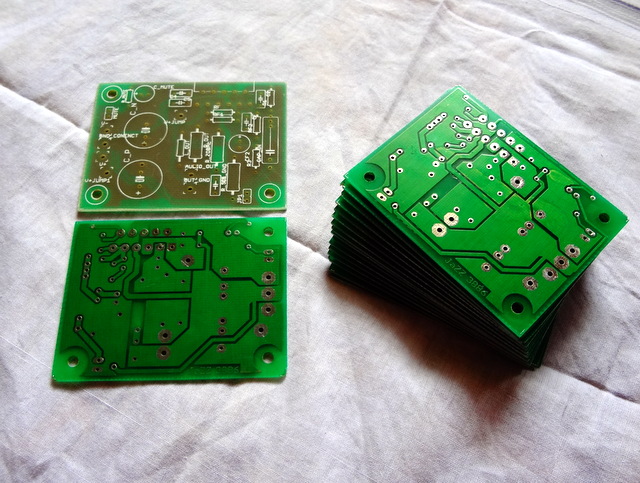
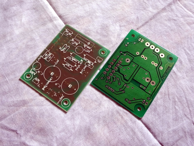
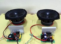
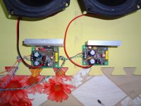
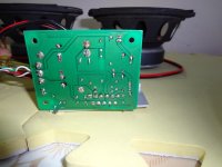
Finished amplifier modules...
One PCB with basic components and second PCB with all extra components (Output inductor and resister, 220pF, 47pF and 22K and with cable provision for mute switch).
One small issue in PCB track was one pad of 220pF was not connected. And another thing was i forgot to apply thermals
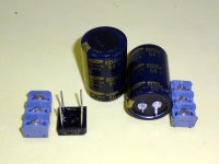
Last image shows simple Power supply using 10 Amp rectifier module and 10,000uF caps.
An externally hosted image should be here but it was not working when we last tested it.
One PCB with basic components and second PCB with all extra components (Output inductor and resister, 220pF, 47pF and 22K and with cable provision for mute switch).
One small issue in PCB track was one pad of 220pF was not connected. And another thing was i forgot to apply thermals
Last image shows simple Power supply using 10 Amp rectifier module and 10,000uF caps.
Attachments
Last edited:
- Status
- This old topic is closed. If you want to reopen this topic, contact a moderator using the "Report Post" button.
- Home
- Amplifiers
- Chip Amps
- Single layer LM3886 planning for PCB samples