Working LM3886 Modules.
LM3886 amp enigma.MP4 - YouTube
DIY Audio Amplifier Blog: LM3886 finished modules
LM3886 amp enigma.MP4 - YouTube
DIY Audio Amplifier Blog: LM3886 finished modules
The entire right side needs a ground plane on the side oipposite the signal traces, or, at the very least, fill everything with a "ground pour" of copper so that there is absolutlely-minimal space between the signal and signal ground conductors, everywhere. Otherwise you will have a good antenna for the hum from the AC Mains and transformer secondary wires, which also need to be tightly twisted, everywhere, so they don't make good transmitting antennas. (See Faraday's Law.)
Also, your small decoupling/bypass capacitors are too far from the power pins. And the +28V one is MUCH too far away. I would also just fill the entire area between +28 and -28 with ground copper.
If you have a 2-sided board, you are definitely not taking advantage of it. ALWAYS use a ground plane, covering one whole side, if you are able to have a 2-sided board. In this case, you will keep the signal and power grounds separate, of course.
That is never going to happen. A good antenna for 50Hz, made from a 2inch wire some 10inches away from a proper built mains transformer?Otherwise you will have a good antenna for the hum from the AC Mains and transformer secondary wires, which also need to be tightly twisted, everywhere, so they don't make good transmitting antennas. (See Faraday's Law.)
I've never used a ground plane or even a ground ring for an LM3886 amplifier, I never needed it. I even built one "in the air" without a PCB. No hum.
The pcb design shown is just fine. Perhaps the 100n decoupling caps could have been closer to the power pins, but I don't think they're "much too far".
Also I would have put a 10ohm resistor between the power and signal grounds.
You don't need a 2layer PCB.
You don't need a Ground Plane.
You don't need any pour fill.
Get the traces for every FLOW & RETURN pair very close together.
That reduces the loop area. That is by far the most important parameter: LOW LOOP AREA.
Of course. But the best ways to accomplish LOW LOOP AREA are, in order from best to worst:
1) 2-sided pcb with ground plane opposite signal traces
2) 1-sided with copper pour to fill ground around signal traces and pads and under signal components
3) 1-sided with existing signal and signal ground traces moved closer together.
That is never going to happen. A good antenna for 50Hz, made from a 2inch wire some 10inches away from a proper built mains transformer?
I've never used a ground plane or even a ground ring for an LM3886 amplifier, I never needed it. I even built one "in the air" without a PCB. No hum.
The pcb design shown is just fine. Perhaps the 100n decoupling caps could have been closer to the power pins, but I don't think they're "much too far".
Also I would have put a 10ohm resistor between the power and signal grounds.
It can and does happen. There are many examples on this forum where tightening such loops eliminated the audibility of 50 Hz hum, which, by the way, is usually due to similarly-gaping loop areas in the AC and transformer WIRING, not from the transformer itself.
Please don't confuse this with RF antenna concepts and wavelength considerations. This is a simple application of Faraday's Law (Maxwell's Equations): Any time-varying magnetic field will induce a corresponding time-varying current in any conductive loop, in proportion to the area enclosed by the loop and the intensity of the field. (Actually there's a line integral of the field, around the loop, involved, et al. But lowering the loop area is the best thing to do to the loop.)
The fact that YOU have "never needed it" is meaningless, in this context. There WILL ALWAYS be currents induced in the input loop that WILL induce voltages across the input resistor which WILL aroithmetically sum with the input voltage, for EVERY electromagnetic field that is ever present, whether it's 50 Hz or RF.
The ONLY question is HOW SIGNIFICANT the effects might be, but we know that it is possible for them to become audible. MINIMIZING those effects is the best we can do. You are saying that should not be done, even though it would then cost nothing extra to build.
The fact that bypass caps should be within no more than a couple of MILLIMETERS from the power pin is a VERY WELL KNOWN recommendation that appears THROUGHOUT the technical literature and many IC manufacturers' Application Notes. If you want to be able to disagree, then show YOUR calculations of the maximum acceptable distance, so we can look for your math error.
You seem to be arguing against accepted best practices. If you believe that the effects being considered would ALWAYS be insignificant, that might be at the edge of being a reasonable position to take, if you had some valid way to back up your position. Otherwise, I believe you should not risk confusing any less-technical readers, here.
Last edited:
Yeah, perhaps in my case the law applied for both inverting and non-inverting input traces and they've got cancelled by the excellent cmrr.
Thanks for clarifying things in your last post, makes more sense for those of us who finished school in the past millennium. But I still believe that if you place and route carefully your stuff in your amplifier case then it will be all-right.
I've never seen a commercial amplifier use a ground plane, but I've seen a lot of boards using ground traces closely guarding long signal traces.
Yeah, perhaps in my case the law applied for both inverting and non-inverting input traces and they've got cancelled by the excellent cmrr.
Thanks for clarifying things in your last post, makes more sense for those of us who finished school in the past millennium. But I still believe that if you place and route carefully your stuff in your amplifier case then it will be all-right.
I've never seen a commercial amplifier use a ground plane, but I've seen a lot of boards using ground traces closely guarding long signal traces.
@ ceteras,
I agree. If you keep the signal and signal ground traces close together, everywhere, and maybe also extend the signal ground under series components that interrupt the signal trace, there shouldn't be any significant problem, except maybe if there was some high-enough-energy high-enough-frequency stuff around, some time.
Last millenium? Yeah, I got out of undergrad in 1978. And rust never sleeps, which seems like quite an understatement; more like "Rust Gone Wild". I've been trying to learn and re-learn EE stuff, and especially the electronics-related parts of it, and also the electronics realities that they didn't teach me in school.
As far as my loop-area fetish goes, I do realize that it often will appear to make very little difference. But beyond 50/60 Hz, which is very-often a severe problem in DIY equipment, due to poor or non-existent lead-dress for example, the EME (Electromagnetic Environment) has become much more cluttered, and is getting worse. And we can't predict who will attempt to build and use the equipment from on-line schematics, or in what type of environment it might be used. So I believe there are good-enough reasons for pushing to make things "good enough".
I have a hunch that RF is a lot more of a problem than most DIY audio builders (and designers) imagine it is. I'm not worried about demodulated AM radio coming out of the speakers. That would at least be obvious. What I worry about is the more-subtle effects that RF can have, such as when it gets rectified to DC-ish and changes ICs' internal operating points. Many DIYers might never realize that their system's performance was compromised. And the effects could also change with time or location. That whole scenario has a rather-tragic quality, to me, especially when it could have been easily avoided.
Anoither common scenario that I hate to have to observe or think about is when the "subjectivist tweakers" are way-over-involved in tweaking or debating the merits of tweaking some component or configuration change, but their layout and/or design has one or more significant problems of the sort that I often harp on, especially when what they are changing could be interacting with its effects.
I used to also always try to prod people here to insert RF low-pass filters, for their inputs, at the least (and outputs, and DC power inputs, often). But (possibly to everyone else's relief) I can only focus on so much at one time. Lately, I've been thinking a lot about capacitors, for both decoupling and linear power supplies, and the ramifications of their connection configurations. In the past, I also pounded on "star grounding" and conductor parasitics a lot.
I guess I need to collect a list of all of the "dos and don'ts" that I have spent so much time trying to stress, in many different threads, and put them all in one place, so I can just post a single link instead of typing so much.
Sorry to have blathered-on about all of that, for so long.
Regards,
Tom
Last edited:
need help
sir , can you check my pcb layout and schematic i think it's wrong something .
An externally hosted image should be here but it was not working when we last tested it.
An externally hosted image should be here but it was not working when we last tested it.
sir , can you check my pcb layout and schematic i think it's wrong something .
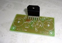
Got PCBs for my second design of LM3886 PCBs. Really happy to see the fabricated PCBs. Kind of a dream come true")
Do You have a pic of this desing, at the printed side?
Looks better than the other one at least.
- Status
- This old topic is closed. If you want to reopen this topic, contact a moderator using the "Report Post" button.
- Home
- Amplifiers
- Chip Amps
- Single layer LM3886 planning for PCB samples