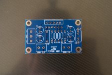
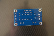
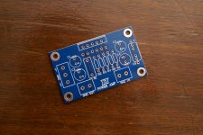
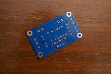
Amplifier PCB pictures.
Hi guys:
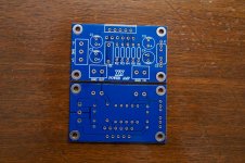
I finally received the amp and psu boards yesterday. Here, I'm posting pictures of the front and back. They are not sharp because I didn't want to use flash, but I think they are good enough to see the cards layout.
I have a few questions:
The instructions that came with the amp boards is confusing. It says that these boards can be used individually or in parallel connection.
It says that when used individually, or "one piece mode" as it literally says on the sheet, the R1 resistor doesn't have to be installed, use a jumper cable instead, and leave the K point of the board alone. The K point is an additional hole by the input capacitor.
Is this the mode I will be using to create a stereo amplifier with one board for each channel, or will it be the "two pieces mode"?.
The "two pieces mode" or parallel is described in the sheet as needing the R1 resistors on both boards, K point parallel connection, boards outputs terminals in parallel connection and only use one input from either board, at least, this is the way I interpret what is written on the sheet.
Please clarify these concepts for me...
The kit came with the terminal connections for each board, 6X 100uf 50V, 2X 22uf 50V, 2X LM3886TF, 2X 0.1 Ceramic resistors, 6X 22K and 4X 1K resistors and 2X 1uf Wima input caps.
I ordered 6X Nichicon KT 100uf 50V, 2X Nichicon Muse ES 22uf 50V (the ones that came with the kit look really cheap, low quality) and 2X Audiophiler MKP 4.7uf 400V capacitors to replace the ones that came with the kit.
Again, your help, comments and suggestions is greatly appreciated.
Hi guys:
I finally received the amp and psu boards yesterday. Here, I'm posting pictures of the front and back. They are not sharp because I didn't want to use flash, but I think they are good enough to see the cards layout.
I have a few questions:
The instructions that came with the amp boards is confusing. It says that these boards can be used individually or in parallel connection.
It says that when used individually, or "one piece mode" as it literally says on the sheet, the R1 resistor doesn't have to be installed, use a jumper cable instead, and leave the K point of the board alone. The K point is an additional hole by the input capacitor.
Is this the mode I will be using to create a stereo amplifier with one board for each channel, or will it be the "two pieces mode"?.
The "two pieces mode" or parallel is described in the sheet as needing the R1 resistors on both boards, K point parallel connection, boards outputs terminals in parallel connection and only use one input from either board, at least, this is the way I interpret what is written on the sheet.
Please clarify these concepts for me...
The kit came with the terminal connections for each board, 6X 100uf 50V, 2X 22uf 50V, 2X LM3886TF, 2X 0.1 Ceramic resistors, 6X 22K and 4X 1K resistors and 2X 1uf Wima input caps.
I ordered 6X Nichicon KT 100uf 50V, 2X Nichicon Muse ES 22uf 50V (the ones that came with the kit look really cheap, low quality) and 2X Audiophiler MKP 4.7uf 400V capacitors to replace the ones that came with the kit.
Again, your help, comments and suggestions is greatly appreciated.
Attachments
It says that when used individually, or "one piece mode" as it literally says on the sheet, the R1 resistor doesn't have to be installed, use a jumper cable instead, and leave the K point of the board alone. The K point is an additional hole by the input capacitor.
Is this the mode I will be using to create a stereo amplifier with one board for each channel, or will it be the "two pieces mode"?.
Yes.
That mode is used to create a mono amp that operates into a current-hungry load, e.g. a subwoofer with low impedance.The "two pieces mode" or parallel is described in the sheet as needing the R1 resistors on both boards, K point parallel connection, boards outputs terminals in parallel connection and only use one input from either board, at least, this is the way I interpret what is written on the sheet.
Thank you, Pacificblue.
Then, I need to solder all the parts into the boards with the exception of the ceramic resistor that goes in the R1 space, and instead I'll put a "jumper cable" there joining the two terminals together, correct?.
In the C5 input capacitor space there are 4 holes in the inside, 2 on the outside, one is the K point which I don't need to worry about, so there are 5 holes left, what holes do I use to solder the capacitor in?.
Thanks again...
Andrew:
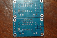
I am posting 2 more pictures plus the diagram for this input board.
Here, the specifications as posted by the seller:
Audio input selector module board, with 12V DC voltage regulator.
This item has been assembled, and electrical test passed.
4 Dual channel input, 1 dual channel output.
Led indicator for each relay channel.
Power Supply: 11 to 22V AC.
or 15 to 32V DC.
Regulator output: 12V DC / 1 Amp.
High quantity terminal block, easy connection wire.
FR-4 Fiber glass PCB ( Double Layer ).
Japan TAKAMISAWA signal relays.
Rotary switch wire length 300 mm (11.8 inch).PCB thickness: 1.6mm (0.063 inch).
Size: 100mm(L) x 50mm(W) x 38mm(H), (3.94 x 1.97 x 1.5 inch).
The relay board is missing a very important part, the freewheeling diode across the relay coils! A big mistake!
C5 the input DC blocking capacitor has two groups of 3 pads. Check that each group are connected together. I think I can see a blue coated trace between each.
This allows you to fit many sizes of DC blocking cap, from 0.2" to 0.6" pin pitch. This suits MKT, MKC, MKS, MKP, FKS, electro etc. FKP may be too big to fit. FKP can go >1.1" pin pitch.
This allows you to fit many sizes of DC blocking cap, from 0.2" to 0.6" pin pitch. This suits MKT, MKC, MKS, MKP, FKS, electro etc. FKP may be too big to fit. FKP can go >1.1" pin pitch.
There is no provision for an output Zobel.
Use the locations of R1 and the speaker terminal to fit an R+C Zobel.
R1=2r0 to 10r
Speaker terminal=47nF to 220nF.
Add the other half of the Thiele Output Network, the R//L, off the PCB. R=2r0 to 10r L=0.5uH to 1.5uH
Insert a thick copper wire in this pad first, The top end of R1, nearest the output PIN.
Attach R1 to the copper wire.
Take the speaker output from the top end of R1. Attach the speaker wire to the copper wire. I suggest you fit the speaker wire on the bottom side.
You could bend over the top side of the copper wire to lie on top of the output PIN. Solder this connection. But fit a temporary tab heatsink next to the package since quite a bit of heat will try to travel along this PIN during soldering.
Last edited:
AndrewT:
I really appreciate your help, it is more than obvious the high level of knowledge you possess in this matter, and it is very nice to see that you, and most others here, are so willing to share it.
Now, what you write here I have to read few times before I start digesting what you mean because my level of knowledge is the equivalent to 1st grade elementary school and you guys are all PhD.
Please tell me if this is what I need to get to do what you recommend in the two PCB's:
2X 1.5uH axial lead inductors.
4X 10 Ohm resistors
2X 220nF capacitors (What type????)
2X 1nF capacitors (What type????)
Thank you.
I would buy a small range of components, probably in quantities of 10s if I were starting out.
Now I tend to buy in 100s and multiple values of the cheaper components.
Think about changing the BOM to
100 10r 600mW 1% metal film resistor
10 47nF 50V, or 63V, or 100V, cheap film capacitor
10 100nF ditto
10 220nF ditto
100gm or 500gm reel of 1.2mm diameter enameled copper wire.
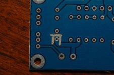
I see 4 pads connected to the bottom side common ground.
Look and see that C4 -ve pin is connected to the common ground.
If you are building a single channel or monoblock then this connection demands that the Main Audio Ground (MAG) must be on the PCB.
If you want the MAG to be elsewhere or you intend to have more than one channel in the chassis then that C4 must be cut from the common ground.
Carefully cut the three trace bridges. Leave the pad intact. The Signal Ground will now be made at the GND terminal next to the IN terminal.
Now I tend to buy in 100s and multiple values of the cheaper components.
Think about changing the BOM to
100 10r 600mW 1% metal film resistor
10 47nF 50V, or 63V, or 100V, cheap film capacitor
10 100nF ditto
10 220nF ditto
100gm or 500gm reel of 1.2mm diameter enameled copper wire.
I see 4 pads connected to the bottom side common ground.
Look and see that C4 -ve pin is connected to the common ground.
If you are building a single channel or monoblock then this connection demands that the Main Audio Ground (MAG) must be on the PCB.
If you want the MAG to be elsewhere or you intend to have more than one channel in the chassis then that C4 must be cut from the common ground.
Carefully cut the three trace bridges. Leave the pad intact. The Signal Ground will now be made at the GND terminal next to the IN terminal.
Last edited:
Cuts on C4 (-) pictures.
Andrew:
It took me a long time to realize what you were saying. I had to do some research and luckily I found another thread about the same issue in the same exact board where you instructed another guy to do the same, and he was very fast to get the idea and very nice to include pictures, that helped me a lot.
Please check my pictures now and tell me if this is right, it should be according to that previous thread I mention above. I used a Dremel with a cutting wheel, it was very easy, I was extremely careful not to ruin the board, but it only took two seconds at the most to isolate the pad with very light pressure.
I used my multimeter to measure continuity from the modified pad to GND OUT, GND IN and the V- GND V+. The pad used to show continuity in ALL GND pads before the cuts, now it only shows continuity with GND IN, is that correct?.
Thank you very much, Andrew, after googleing and browsing for more information regarding this mods, I realized that you have helped many people, that's very nice of you.
I have some more questions, but I'll save them for later, I just want to make sure I did this right.
Thanks again.
Attachments
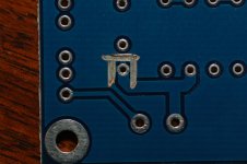
Did I ruin the PCB's?
I did it this way because in that previous thread you suggested not to do it so closely to the pad to avoid damaging it.
Even though you can still see the three little bridges, the pad is now totally isolated from V- GND V+ and GND OUT, there is only continuity between the pad and the GND IN. Is this correct?.
This cuts may look huge in the picture, but I applied very light pressure, just enough to isolate the pad from the GND OUT and DC GND, they are long because the only cutting wheel I have is like 25mm in diameter, I guess I could've done a much better and precise job using a much smaller cutting wheel, also my eyes are not as good as they used to be, these PCB's look big in the pictures but they are about half the size of a credit card, the pads are very small and the holes in them are about 0.6mm in diameter.
If it wasn't because you had gone through this in that other thread and the guy was nice enough to post pictures, it would've taken at least 80 replies from you for me to be able to digest this and finally see those three bridges.
Please tell me if I should do additional continuity tests to determine any damage to the PCB's, or if even though not perfect, these cuts are OK...
Thanks again, Andrew.
- Home
- Amplifiers
- Chip Amps
- Bought a XY LM3886 Kit.