I have a radio which uses BA5417, and have enormous gain(45db), thus have audible hiss & easily amplifies RF, chip noise, etc. My idea is to reduce the gain of the amplifier, maximize the Negative Feedback, but I have no idea how to reduce the gain.
The radio's circuit is slightly different than BA5417 original datasheet's circuit, so I couldn't find the NFB divider.
I'm learing from discrete amplifier, but i would make use of this circuit with the minimum modification. (to preserve the board, avoid changing of board)
If i'm not wrong, changing only the gain(NFB) would usually changes the Iq & DC offset, is there compensation i need to add ?
The radio's circuit is slightly different than BA5417 original datasheet's circuit, so I couldn't find the NFB divider.
For convenient of reference :
http://www.datasheetcatalog.org/datasheet/rohm/ba5417.pdf
I'm learing from discrete amplifier, but i would make use of this circuit with the minimum modification. (to preserve the board, avoid changing of board)
If i'm not wrong, changing only the gain(NFB) would usually changes the Iq & DC offset, is there compensation i need to add ?
Attachments
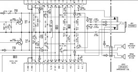
Yes it does look like R110 and R111 are used for adjusting the gain. Though the values don't seem to make sense for a gain of 45. I'd have thought a 1K resistor in the place of the 270 should bring the gain down to about 29 times. but using a simple calculation for the 30K internal resistor with 45 ohms internal + 270 ohms external for the shown schematic seems to imply a gain of 95 times not 45 (or were you talking db?, that would be about 40db).
I'm uncertain about the dc offset but since there are feedback capacitors fitted (c126 and C130) the gain at dc should be zero, so I don't think that changing the gain should have any effect on the dc offset.
Tony.
I'm uncertain about the dc offset but since there are feedback capacitors fitted (c126 and C130) the gain at dc should be zero, so I don't think that changing the gain should have any effect on the dc offset.
Tony.
so which component is most convenient to tweak with minimum alteration to the board would be ?
yes, i was talking about 45dB, so it seems it was between those number. But the weird thing is the BTL method didn't state its gain there. So only could assume anyway.. but i could swear the gain is very high.
yes, i was talking about 45dB, so it seems it was between those number. But the weird thing is the BTL method didn't state its gain there. So only could assume anyway.. but i could swear the gain is very high.
It's a Sony from the '90s, huh?
Apparently the amplifier that is inverting in the datasheet BTL config is used in non-inverting mode and vice versa.
Since BTL amps aren't exactly transparent to me, I resorted to drawing and simulating this one. Interesting. You get about 45 dB of gain for the speaker and 39 dB for headphones. Speaker gain can be increased further by decreasing R112, but in order to get basic gain down, you'd have to increase R110. (Same for R2xx counterparts.) Since there already are open-loop-gain draining caps present, the risk of oscillation should be relatively low as long as you don't overdo it (going down to about 20 dB should be quite feasible).
So how much gain do you want for headphones and speakers, respectively? Are you satisfied with headphone driving? (100 ohms of output impedance is on the higher side of things by hi-fi standards, and those coupling caps aren't too huge.)
Last edited:
Hard to tell. Try a 3k3 and see what happens. Do you have anything that could be used to probe for RF up to a few MHz? If the chip gets warm and power draw is up, you obviously have oscillation, but it can be much more subtle while still degrading performance.
With a 3k3 for both R110 AND R111 (you need to get noise gain down for both amplifiers for hiss to be reduced effectively), you should be getting about 26 dB of voltage gain... if that works out well, you have lost almost 20 dB of hiss, which tends to be a BIG improvement subjectively. Distortion will also be reduced accordingly.
Try that and see how it works out. A bit of gain to spare tends to be quite useful at times.
Since you mention 1 Vrms, I suppose the source is a DAP?
hm... I agree with you that a spare is sometimes a good thing. Hm.... so i'm going to increase the value of 270 ohm to 3k3 ? quite big value. Will try out on next week (temporarily occupied now)
Just to ask, if only change R110 but not R111, or vice versa, what will happen ?
hm.... First, I will try out with a variable resistor first. I have quite much of spare 2k7 resistor, so if it is near that number, i will use that.
Just to ask, if only change R110 but not R111, or vice versa, what will happen ?
hm.... First, I will try out with a variable resistor first. I have quite much of spare 2k7 resistor, so if it is near that number, i will use that.
R111 only: Not much of a difference, gain goes up by <1 dB.Just to ask, if only change R110 but not R111, or vice versa, what will happen ?
R110 only: Gain goes down by 20 dB, but since the other amp is still running at 40 dB of gain, reduction of hiss (and distortion) is limited to a maximum of 6 dB.
Neither really is what you want.
I figured 2k7 was a bit of an odd value, but if you've got plenty of those, it should be fine...hm.... First, I will try out with a variable resistor first. I have quite much of spare 2k7 resistor, so if it is near that number, i will use that.
lol..... 2k7 was an odd number, i didn't knew that...R111 only: Not much of a difference, gain goes up by <1 dB.
R110 only: Gain goes down by 20 dB, but since the other amp is still running at 40 dB of gain, reduction of hiss (and distortion) is limited to a maximum of 6 dB.
Neither really is what you want.
I figured 2k7 was a bit of an odd value, but if you've got plenty of those, it should be fine...
well.... the concern i'm asking because I don't have dual gang potentio to adjust it, so I want to adjust one at the time, or should i just replace those (R110/111, R210/211) with 2k7 directly ?
I know slightly how to use simulator, but how could you simulate BA5417 ? it was quite an old model...
The gain is given by the speakers attached ! 
But...I think that the problem to be overcame is to be found where
Guitar 89 has pointed it : if the amp picks some unwanted signal , maybe
that is to be investigated .
I think that great corporations like Sony make such indestructible products if they are not worked beyond their purposes
My English today is...TOO MUCH !!!
If the socalled DAP is a cheap PC not engineered for good sound , that is a cause.
Poor supply ( decoupling ) and some junk traveling along the lines .
Because...the gain is never enough !! Some Gain-BW product may tell the truth ..
But...I think that the problem to be overcame is to be found where
Guitar 89 has pointed it : if the amp picks some unwanted signal , maybe
that is to be investigated .
I think that great corporations like Sony make such indestructible products if they are not worked beyond their purposes
My English today is...TOO MUCH !!!
If the socalled DAP is a cheap PC not engineered for good sound , that is a cause.
Poor supply ( decoupling ) and some junk traveling along the lines .
Because...the gain is never enough !!
Some Gain-BW product may tell the truth ..hey yo, Mr. pico tony ! Well.... i think it wasn't power supply problem, just some hissing from the chip itself.
I think also contained some RF/EMI noise, since the enclosure itself is not shielded.
The gain is also too high for me. At least what I thought is to increase NFB for better THD, etc.
I think also contained some RF/EMI noise, since the enclosure itself is not shielded.
The gain is also too high for me. At least what I thought is to increase NFB for better THD, etc.
So you may try that odd value resistor -2K7 - at the input of the amp , to form a an RC filter together with a 1nF cap...well ,I see there just one already
3K9+3n3 ! Did you remove the emitter of the transistor at the input joint ?
I see many 'Cdp tweakers' often remove the mute transistors at the output
Now ; you reported the fact that the amplifier is not shielded ...shield it !!
Perhaps the whole pcb containing amp's circuit is too big because it houses also radio and cd traces and components ? Rip it !
I remember that IC ( Ba 5417 ) being very ( fairly )good , capable of producing
a loud bass...with 4Ω woofers and 2nd order lowpass .
Bye !!!
sgrossklass, I have done trying with 2.7k resistor, and no problem seems so far (tested few minute only though)
The hiss is reduced significantly, nice sound is retained though. However, The amplifier isn't sound nice when using direct PC soundcard (compare to other amplifier), however when i use a good quality external soundcard, its sounds nice.
Does this have relation to input impedance ? Maybe the soundcard was driving the amplifier hard ?
I'm also thinking to bypass headphone, how should I connect ?
Could I just bypass C234, R219, L201 ? means can I connect positive side of C134/234 to positive post of each speakers ?
(My main purpose is because those component leave the main circuit very far, wanted to dispose of them for smaller board)
Attachments
Measure it and compare to the measurement/s from your other source/s.............. Maybe the soundcard was driving the amplifier hard ?..........
- Status
- This old topic is closed. If you want to reopen this topic, contact a moderator using the "Report Post" button.
- Home
- Amplifiers
- Chip Amps
- ba5417: adjust gain