Hi
I am trying to make chipamp with LM3886 output 30W RMS per channel, my config as under
Transfo 200VA , 20-0-20 secondaries unregulated power supply with Capacitor 10,000uF/63V on each power rail
Speaker 8 Ohms
Gain 20X
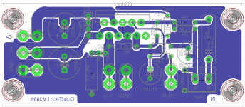
Attached picture of single sided PCB layout with component placement. Are there any deficiencies ? any improvements needed ?
Thanks for your time
Yatin
I am trying to make chipamp with LM3886 output 30W RMS per channel, my config as under
Transfo 200VA , 20-0-20 secondaries unregulated power supply with Capacitor 10,000uF/63V on each power rail
Speaker 8 Ohms
Gain 20X
Attached picture of single sided PCB layout with component placement. Are there any deficiencies ? any improvements needed ?
Thanks for your time
Yatin
Attachments
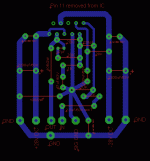
why does everyone make the same layout mistake
for some reason nearly all chip amp pcb layouts I've seen mistakenly go for "symmetry" in the pwr routing with +.- on opposite edges of the board, as far apart as possible - can't get more wrong from a circuit operation point of view
I'd put pwr traces, PS caps on the same (left) edge of the board, move the gnd trace from the left inwards
look at current paths, minimize loop areas - this means pwr wires, traces need to be as close together as possible, as well as close to gnd
the "star gnd" is poorly conceived - you should really want input signal ref, feedback network gnd and load gnd to be the "star" point - the jumpers to the gnd "racetrack" give many loops, paths for "gnd contamination" from the Class B currents that look half-rectified in the separate +,- ps wires and ps cap gnd return paths
for just a single stereo build I'd just do point-to-point "air wire" or with at most a perf board - can be done really well and give better performance than many PCB layouts I see
the only reason I can see for a PCB is if you want multichannel or active XO - then I'd think about system level power, gnd routing - probably add a op amp differential receiver for signal input
and with the extra parts 2-layer becomes more attractive, gives better routing - I really don't care to work with home etched boards, of course a small batch from a PCB manufacturer that has prototyping deals only costs about what I now consider a "nice" restaurant dinner
Last edited:
Too cool! That's more like the real gaincard.
Too cool! That's more like the real gaincard.
But nowhere near good enough heatsinking to run at full rail voltage.
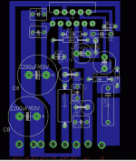
Changed Layout
Thanks for detailed reply JCX, I wanted it to be on PCB because threre are other PCBs like Speaker Protection and Bass & Treble control
Would this be a better layout sonically ?
Power ground and signal grounds are in separate traces tied via 10R/2W resistor
Thanks
Yatin
Thanks for detailed reply JCX, I wanted it to be on PCB because threre are other PCBs like Speaker Protection and Bass & Treble control
Would this be a better layout sonically ?
Power ground and signal grounds are in separate traces tied via 10R/2W resistor
Thanks
Yatin
Attachments
Last edited:
Hi Yat.
the Power traces are far better located now.
Try to thicken up the thin parts of those traces. They do have to pass high transient currents, or at least as large as the 3886 will allow. Look at PIN2. It is not connected. You can use this spare PCB area to thicken traces.
Remove the 90degree internal corners from your traces. Imagine your electrons as yourself driving around a race track (Indianapolis). Round the corners.
Re-trace the inputs to PINs 9 & 10.
They are too far apart. Keep them as a close coupled pair from the two input terminals all the way to the two input PINs.
Keep the Signal Return separate from the Power Ground.
This is very important if you adopt the same PCB for a multi-channel amplifier. In monoblock you can get away with Main Audio Ground on the PCB, but not in multi-channel.
Finally,
you may find that very small ceramic caps make for excellent power pin decoupling. These can be fitted much closer to the Power PINs than those big 0.2" pin pitch film caps shown.
Last edited:
But nowhere near good enough heatsinking to run at full rail voltage.
Duly noted.
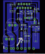
I would still see what swapping + pwr and gnd looks like
you would have to route V+ between V- PS cap pins but you probably have the room - even if you have to "neck down" the trace as it passes between the pins
the gnd at the board entry is about as "clean" as it can be and should be the signal gnd ref - unless you put a diff receiver cirucit on the pcb to allow a completly separate signal gnd
Thanks Anderw for the detailed reply
Yes the horizontal 10R is wound over to form inductor L, missed to put L in the name
Pwr traces are 4mm wide at arrowest, traces to pin 9 & 10 are 1mm thick will they be enough ?
I will modify layout not to have bends at right angles
Thanks to all
Regards
Yatin
Yes the horizontal 10R is wound over to form inductor L, missed to put L in the name
Pwr traces are 4mm wide at arrowest, traces to pin 9 & 10 are 1mm thick will they be enough ?
I will modify layout not to have bends at right angles
Thanks to all
Regards
Yatin
One more detail . . .
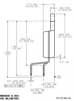
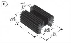
It looks like the board extends beyond the back row of pins too far to allow mounting the chip to a heatsink. According to NS's data sheet you have 4.3mm from the center of the back row of pins to a line parallel to the back of the chip. See the 1st picture.
Also, keep in mind that if the copper goes right up to the edge of the board, the copper will be exposed. It looks like your negative rail goes right up to the edge which will be against the heatsink.
It seems kind of late now, but you can probably get away with using a heatsink which sits on top of the board, like the Ohmite RA-T2X-64E (2nd picture). This allows you to put your chip anywhere you want on the board. That's what I'm using right now. I'm using +/-25V rails, driving 4R speakers and I've never had overheating problems.
Good luck.
-Byron
Attachments
C1 and C2 are too far from the chip's pins. I would remove the "stub" that comes down to C1 and extend the gnd trace toward the chip, instead, then turn C1 90 degrees and put it right next to the chip. At the same time, move C2 upward toward where C1 was, so it's in line with the pin it connects to, and as close as possible. A millimeter or two makes a difference, with those small-value capacitors. If possible, put them underneath the board, so they can be connected RIGHT AT the power pins.
Your main smoothing caps, C6 and C8, would also be better if placed as close to the chip pins as is practical. There is room to easily move them a lot closer than they are.
I would also minimize the spacing between the power and ground traces.
It would probably enable the design to be better and much easier to implement if you just used a two-sided PCB but left one side almost all unetched, for a ground plane. You might have to make short traces to get out from under certain components, like the large caps, to be able to solder on the top side ground plane. But it should still be much better and much easier to lay out. You would have to etch or otherwise remove a little copper on the gnd plane side, from around the component-lead holes to the other side. But that would be simple enough.
- Status
- This old topic is closed. If you want to reopen this topic, contact a moderator using the "Report Post" button.
- Home
- Amplifiers
- Chip Amps
- Help on LM3886 PCB Routing