gootee - no i havent - not yet anyway. i wanted to touch base with you folks to see if the PCB would help you at all - and then move forward when a consensus was reached as to improvements ")
dan - thanks for the input - much appreciated.
ian - thanks - what problems (other than what dan has eluded to) would you advise exist - i welcome your feedback also please.
thanks guys
dan - thanks for the input - much appreciated.
ian - thanks - what problems (other than what dan has eluded to) would you advise exist - i welcome your feedback also please.
thanks guys
Ah, but I think that you will see a power circuit difference.
The solo non-inverting LM1875 probably prefers 470uF high performance caps.
However, when we start a pile up, this may need to reduce to 330uF.
If you get in a tangle with layout and need to jumper something or "cable out" then do it to the speaker. The speaker is a member of power star, meaning that the speaker is a "competitor" to the amplifier, and so there's no need of speaker traces running all over the amplifier board looking as if the amplifier were tackled in one of our football games. Instead, it may be very convenient to locate the speaker output component collection onto its own private daughtercard. You have big output resistors, RC and inductor//resistor assembly all for a speaker support circuit. Going about it this way avoids the layout mistake of pushing speaker energy into small signal. After this consideration, you could then join the two boards together for a streamlined look, if you like.
Edit: For example, my point to point build has all of the speaker support circuit onto the speaker jack because it will not fit at my amplifier. Perhaps I should use a daughtercard too, because the speaker support components could perform better if located closer to the amplifier.
Last edited:
many thanks guys for the feedback - much appreciated - i've only been looking into this field for a few months having been interested in it for years, have not done the hard yards so simply don't have the experience.
i had a similar revelation when i woke this morning - simplify via one LM1875, then, add the other sections one at a time. get the layout of the first one right, then, duplicate with the necessary pieces the other two sections.
stay tuned will see what i can muster and learn.
many thanks
i had a similar revelation when i woke this morning - simplify via one LM1875, then, add the other sections one at a time. get the layout of the first one right, then, duplicate with the necessary pieces the other two sections.
this is the key bit i need the help with.learn how to layout a Power Amplifier
stay tuned will see what i can muster and learn.
many thanks
i'd love to hear them gootee.
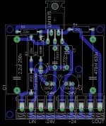
i reviewed the LM1875 datasheet this AM briefly which speaks of layout, and, as per AndrewT's suggestion - started with a brief layout of one amp only.
This ended up with a smaller more compact design, which, seemed to flow with all components in what i think are the right places.
I then duplicated the layout for each next 'section'
As it stands the only tie I have now (or top side of a double sided PCB) is the link between the output of each of the tail of the 150ohm resistors to line out.
Note that the initial 2u capacitor and 100k resistor I will move off the board and to the input at the RCA as I no longer have the room (note PCB is 100mm x 80mm (or 4" x 3.25" for the non playstation generation)
i'll post it up tomorrow as i need some sleep.
thanks AndrewT. with you now. correct it as per a single board layout, ensure it works as per expectations, THEN move on to something that has multiples.
i've built an LM1875 amp before (as a single) - and its marvelous. but not to my own design. which is the key piece thats missing here (as well as the underpinning theory to substantiate component selection, values, and placement criteria)
i've built an LM1875 amp before (as a single) - and its marvelous. but not to my own design. which is the key piece thats missing here (as well as the underpinning theory to substantiate component selection, values, and placement criteria)
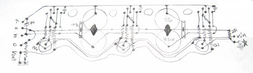
Well, I sketched a compact horizontal layout, but I don't like it since small signal has to jump over v+. After finishing the sketch, it was apparent that the 470uF 50v were just too big so I labeled them 330uF 35v, which is a more sensible size for the board, and the textbook value as well, but I didn't redraw, since there must be a significant amount of room between caps and heatsinks.
*The mysterious circles with no connection are holes for air--to help the caps last.
*For this power circuit, it appears that the sketch is too wide.
*The tiny little caps between V+ to V- directly at each chip are very tiny value ceramic or polyester, about 3.3nF. And at the far left edge, the solo 4uF 250v shown blocks a lot of noise.
The sketch doesn't quite show correct things to do with traces, since some of them are too close and some are wrong thickness. For the appropriate length jump over appropriate size traces, most resistors at the jumper area would have tiny pads and possibly enough room for a 1w resistor, with the speaker output having room for a 5w resistor.
It isn't without benefits. It shows the speaker as a power component, separated far away from small signal input and it gives signal star ground. There is a heck of a lot of room to put in whatever filters you want. It allows flyback diodes added at farthest left to support "alternative" chips not exploding while driving huge woofers. And the compact PCB size is inexpensive.
I will attempt to do better next time:
Please check validity before using.
Attachments
If you want the job done fast:
Vertical layout seems to be a lot more fun with 3 identical copies of a tiny LM1875 single chip amplifier, with all 3 boards turned at 90 degrees so that the connections are all streamlined straight across. . . like the vertical cards and horizontal bus of a mainframe computer. This appears to work with any 3 identical circuit boards, including prefab. With smaller boards, such as postage stamp size, performance should be similar to a point to point build.
Vertical layout seems to be a lot more fun with 3 identical copies of a tiny LM1875 single chip amplifier, with all 3 boards turned at 90 degrees so that the connections are all streamlined straight across. . . like the vertical cards and horizontal bus of a mainframe computer. This appears to work with any 3 identical circuit boards, including prefab. With smaller boards, such as postage stamp size, performance should be similar to a point to point build.

Hello there,
I've amended the layout again based on the components available to me. I managed to get far smaller capacitors (100nf and 470nf) which are rated for 100v which will be sufficient.
I'd appreciate feedback please
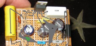
Well, I took your layout and just did this to it:
Star grounding avoids hard forward sound of slamming speaker return current into NFB cap. Notice the absence of suggesting speaker return to amplifier board, although the 0v tap may be used for speaker return.
A pair of 330uF 35 power caps are textbook spec for LM1875--its only the china counterfeit chips that need 220uF 25v and lower voltage (as if TDA2030).
The input cap now has alternative size pads for signal grade electrolytic, most of which are excellent in smaller sizes. But just in case somebody spends a lot more for a lot less quality, RF filtering helps prevent mistakenly large input caps from acting as noise collecting antennas.
The 2.7k can be changed to 3.3k for a normal gain setting, but otherwise the resistor values shown add some support for generic chips.
This board is much too heavy to be supported entirely by the little chip, and so we should probably consider a compact board that's not as full as this. For an LM1875, this board is huge!!
I've included a starfish in the photo to make a point--star grounding.
Attachments
here is the next incarnation based on the original components.

once i understand the additional resistors and cap i'll map out a PCB for you.
- but are you suggest a nomal radial polar cap could go here??
the board as shown above is just shy of 2 inch squared.
i didn't quite understand star grounding. i do now. i'll carry this over to my valve designs as well as they stipulate it in their point to point wiring configs.
many thanks and appreciation for your help
once i understand the additional resistors and cap i'll map out a PCB for you.
i interpret this by sharing the same ground with other components to stop the slammingStar grounding avoids hard forward sound of slamming speaker return current into NFB cap
i did - and i find this interesting. the speaker has to have (with the exception in the case of the triple setup) a return. what i find truly interesting is the seperation of the 0v ground and the line input ground - why?Notice the absence of suggesting speaker return to amplifier board, although the 0v tap may be used for speaker return.
yep cool with that - although i'd love to actually understand how these are sized for the application (i lack the theoretical context of electronics, apologies)330uF 35 power caps are textbook spec for LM1875--its only the china counterfeit chips that need 220uF 25v and lower voltage
added the additional pad - cool idea. a signal grade electrolytic - this i find EXTREMELY interesting - i have a similar input cap to yours on your little perfboardThe input cap now has alternative size pads for signal grade electrolytic, most of which are excellent in smaller sizes. But just in case somebody spends a lot more for a lot less quality, RF filtering helps prevent mistakenly large input caps from acting as noise collecting antennas.
- but are you suggest a nomal radial polar cap could go here??what is considered 'normal' gain? i pulled the gain back to 21 not to overly stress the device, it was by the default values at 31. yes the resistor values can support the TDA2050 and other seriesThe 2.7k can be changed to 3.3k for a normal gain setting
the board as shown above is just shy of 2 inch squared.
i didn't quite understand star grounding. i do now. i'll carry this over to my valve designs as well as they stipulate it in their point to point wiring configs.
many thanks and appreciation for your help
dan
here you go ;
here you go ;
An externally hosted image should be here but it was not working when we last tested it.
Hi,
R1 is in the wrong position.
Remove it. C8 connects from Signal Hot to Signal Return.
Add R1 in series with C1, but before the tapping for C8.
I note you have labeled the Signal Return Differently from the Main Audio Ground. Well done.
Add a pair of inverse parallel diodes across R8. The diode passes Fault Current to blow a Fuse if faulty equipment is connected to your input RCA.
I think R10 (0r22) is going to be too high. BTW, never omit the leading zero in values less than unity.
The combination R2 & C2 is unusually high with RC ~400ms. This will not do any harm. But some adjustment may give lower noise and/or smaller/cheaper components
Last edited:
- Status
- This old topic is closed. If you want to reopen this topic, contact a moderator using the "Report Post" button.
- Home
- Amplifiers
- Chip Amps
- Need help with Triple Parallel LM1875 dynamics amplifier.