My_Ref Fremen Edition
This thread starts to discuss a variation of Mauro Penasa's My_Ref with this goals:
I've been authorized by Mauro Penasa to proceed with this My_Ref derivate amp.
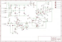
Mauro also pointed out some minor glitches that should have been fixed in the attached schematic.
Also, we will discuss on a better performing LM318's PS (at the moment the schematic include the original zener shunt supply) and, maybe, on possible mods to the compensation scheme.
I've already tried a simple TL431 peer to peer regulator that works and in theory should measure much better than zeners but in practice sounds (much) worse.
On amp's name:
This thread starts to discuss a variation of Mauro Penasa's My_Ref with this goals:
- a more stable and performing amp using SMD parts
- raise LM318's PS voltage thanks to a voltage limiter
- Better PS for LM318
- bigger caps (16mm diameter with both 7 and 5 mm pads) for C1, C2, C9
- large use of SMD components
- all small caps and some critical resistors are still through-hole
- the feedback resistor (R7) can be through hole or MELF
- very small paths thanks to SMD
- ground planes in star configuration
- zener limiter based on schematic 5b from this link (which seems pretty similar to My_Evo one)
- a double diode bridge like in most gainclones (tested by Suburra with great results)
I've been authorized by Mauro Penasa to proceed with this My_Ref derivate amp.
Mauro also pointed out some minor glitches that should have been fixed in the attached schematic.
Also, we will discuss on a better performing LM318's PS (at the moment the schematic include the original zener shunt supply) and, maybe, on possible mods to the compensation scheme.
I've already tried a simple TL431 peer to peer regulator that works and in theory should measure much better than zeners but in practice sounds (much) worse.
On amp's name:
- As part of my nickname the name is an homage to Frank Herbert's Dune novel.
- The official abbreviation for My_Ref Fremen Edition is My_Ref_FE
")
Attachments
Last edited:
Very happy that Mauro is willing to offer a bit of assistance. I was beginning to believe he was just a figment of someones imagination. Hopefully many will post here and enjoy working on the development level of this project.
Thanks again for your efforts - both Dario and Mauro!
Thanks again for your efforts - both Dario and Mauro!
Very happy that Mauro is willing to offer a bit of assistance. I was beginning to believe he was just a figment of someones imagination.
Mauro exists, be sure...
But the fact he kindly asnwered my mail and gave permission doesn't mean he is willing to offer assistance.
Obviuosly if it will ever happen I'll be happy and honored.
Hopefully many will post here and enjoy working on the development level of this project.
I hope so...
Thanks again for your efforts
You're welcome, Bob
I am going to try these on the original Rev C for LM3886 PS
?????? » AD6-11242411B » A6-11242411B » ????? DC24V 1.1A x2 ???????
Do not think there will be a ground problem, but we shall see.
It will also be interesting to see if the EMI will effect the circuit or not. Local EMI radiation seemed to be within standards here.
?????? » AD6-11242411B » A6-11242411B » ????? DC24V 1.1A x2 ???????
Do not think there will be a ground problem, but we shall see.
It will also be interesting to see if the EMI will effect the circuit or not. Local EMI radiation seemed to be within standards here.
...
I've been authorized by Mauro Penasa to proceed with this My_Ref derivate amp.
...
- As part of my nickname the name is an homage to Frank Herbert's Dune novel.
- The official abbreviation for My_Ref Fremen Edition is My_Ref_FE
Dario - great and way cool!
Good luck on the design and layout - I'll try to contribute my 2c from time to time.
I've started running simulations, but the NatSemi LM318 model is an incomplete behavioural model which doesn't model external compensation through the comp pin. I'm trying to find a component-level model which can be modified.
Dario - great and way cool!
Good luck on the design and layout - I'll try to contribute my 2c from time to time.
Hi Siva,
thanks
Your contribution will be precious.
I've started running simulations, but the NatSemi LM318 model is an incomplete behavioural model which doesn't model external compensation through the comp pin. I'm trying to find a component-level model which can be modified.
It would be great!
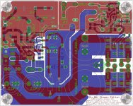
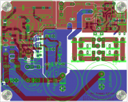
That's a very nice layout. since you're now designing the PCB from the ground up, i thought i'd suggest another way of placing the components. I see you're good at copper pours, so this shouldn't be a problem. One benefit would be that the large capacitors won't be in the way of a screw driver when you try to mount the chip onto the heatsink.
Attachments
Dario,
I'm new to this, so I don't know if I'm reading the color coding correctly. If a thin white border represents isolation from the ground plane, then look at the pads of R10 and R13. I think you have the wrong end isolated from ground. Is R12 isolated?
What are D7 and D8 connected to on the ground end? I see white borders around their pads, too. Am I interpreting this wrong?
I see you've eliminated the bypass cap from C9. There was a lot of discussion about that, so it might be nice to leave the option there if you can fit it in. Other than space, it doesn't hurt anything to have extra pads and a small trace.
You do not want to move the big PS caps, as they provide some physical blocking of AC section from the signal area. I don't know if that's really important for the low noise level this amp exhibits, but why mess with it? We know there are ways to mount the chip after the caps are in place.
Why does the signal input trace now cross underneath R10? Perhaps the input pads should be moved back to be next to C13. Can you put R10 at a 45 degree angle?
There is not much space around R3 if people want to use bulk metal foil resistor with a heatsink there. It's very tight on the old board, and this looks even tighter.
R7 is in the way if C9 is bigger. Is there an extra pad under R7? Hard to see what's going on there.
There is a single pad below R11. I think it says C11.
I'm trying to digest all the changes you made. Sorry I can't help much with the circuit itself.
Peace,
Tom E
That's a very nice layout.
Thanks
i thought i'd suggest another way of placing the components.
...
One benefit would be that the large capacitors won't be in the way of a screw driver when you try to mount the chip onto the heatsink.
When I've first tried to arrange components on the PCB I've tried also that solution but it wasted too much space... and as Madisonears pointed out the possible screening offered by the big smothing caps from both the diode bridge and the relay coil is lost.
BTW I'll check again.
I'm new to this, so I don't know if I'm reading the color coding correctly. If a thin white border represents isolation from the ground plane, then look at the pads of R10 and R13. I think you have the wrong end isolated from ground. Is R12 isolated?
What are D7 and D8 connected to on the ground end? I see white borders around their pads, too. Am I interpreting this wrong?
Hi Tom,
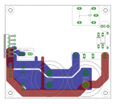
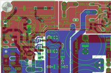
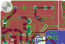
Take a look at the attached detail, the white borders are termal pads (easier to solder and, eventually, desolder)
Red represents the top layer, blue the bottom one.
Darker red are tracks overlapped by the other layer.
I see you've eliminated the bypass cap from C9. There was a lot of discussion about that, so it might be nice to leave the option there if you can fit it in.
Right, I'll check if it's possible the use of a TH cap without disrupting current return paths.
A SMD position is possible and I've added it, as you can see in the attachment.
IYou do not want to move the big PS caps, as they provide some physical blocking of AC section from the signal area. I don't know if that's really important for the low noise level this amp exhibits, but why mess with it? We know there are ways to mount the chip after the caps are in place.
As I wrote above I do agree but I'll do a rapid check, just to be sure.
IWhy does the signal input trace now cross underneath R10? Perhaps the input pads should be moved back to be next to C13. Can you put R10 at a 45 degree angle?
Initially it was so but I've arranged things this way to gain more distance between output ground and R13 and C12.
Input signal cross R10 at 45° and this should minimize the influence.
Not sure on which solution is better (R10 not crossing input signal or R13 and C12 nearer to output ground?).
IThere is not much space around R3 if people want to use bulk metal foil resistor with a heatsink there. It's very tight on the old board, and this looks even tighter.
Unfortunately gainining more space is problematic but I've verified that a small heatsink like the one I've used for RevC fits well and mine gets barely warm.
As you can see in the attachment such heatsink now is indicated in the silk-screen.
R7 is in the way if C9 is bigger. Is there an extra pad under R7? Hard to see what's going on there.
See the pic.
There are two alternatives:
- R7 can be monted on bottom side
- there is a position for an alternate MELF R7 (between R7 and C32)
The use of the MELF R7 shortens a lot the feedback loop.
There is a single pad below R11. I think it says C11.
The 'C11' label is wrongly placed, it refers to the elco below.
That pad is a via between layers.
II'm trying to digest all the changes you made. Sorry I can't help much with the circuit itself.
Any feedback is useful and welcome.
Attachments
Last edited:
When I've first tried to arrange components on the PCB I've tried also that solution but it wasted too much space... and as Madisonears pointed out the possible screening offered by the big smothing caps from both the diode bridge and the relay coil is lost.
BTW I'll check again.
Sorry but, as you can see in the attachment, the radiating tracks of the diode bridge are too near to the 0V zone....
And lack of space is greater...
If the PCB will grow in dimension (but I should buy Eagle Hobbyst Edition... 160€) this option will come back.
Attachments
Last edited:
The current PCB seems to be a nice size. Is C13 really necessary? I have never used an input cap in 30 years. If the DC gain is low enough, then this space is really a waste. If someone needed it, it's easy to connect anywhere in the input line between connector to PCB with any type you want. There are so many caps that are too big to fit on the PCB anyway.
The current PCB seems to be a nice size. Is C13 really necessary? I have never used an input cap in 30 years. If the DC gain is low enough, then this space is really a waste.
In this design the C13 input cap is tightly connected with C9, it can't be omitted without impacting on bass performance.
There are so many caps that are too big to fit on the PCB anyway.
Quite all... in fact the cap I recommend in my BOM will fit only outboard as in the attached picture:
Attachments
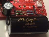
It's my understanding that this is basically providing additional subsonic filtering (at least that is what was also previously described in the technical explanation). If it really creates a problem, then the problem would be elsewhere and system specific.In this design the C13 input cap is tightly connected with C9, it can't be omitted without impacting on bass performance.
...
The point is, if it has to be mounted off board for best performance, why let it take up so much PCB space? All we probably need is two pads that will allow a small cap to be mounted vertically, this way we can save space for other valuable stuff.
PS. Try moving that cap in the pic around and see whether you notice a difference in sound.
Last edited:
move C13 off board. And use it to connect the RCA/phono/input terminal to the PCB.
Probably it's a good idea to do it... I'll check
Then along side you can have a DC input socket as well as the AC input socket.
If I understand correctly you're suggesting to place two input sockets, one that goes directly to the input net (so the coupling cap can be completely off board) and another connnected to two pads that allows mounting a tiny onboard cap, right?
no.
Look back at Jen's Leach clone.
One of the input pins bypasses the DC blocking cap.
So a 3 pin connector...
Not much different from what I wrote but I get it
Thanks, I'll take a look.
Last edited:
If it really creates a problem, then the problem would be elsewhere and system specific.
Hi Soongsc,
it don't create any problem, simply it is part with C9 of the high-pass filter to avoid DC.
The point is, if it has to be mounted off board for best performance, why let it take up so much PCB space? All we probably need is two pads that will allow a small cap to be mounted vertically, this way we can save space for other valuable stuff.
I'm thinking about it.
PS. Try moving that cap in the pic around and see whether you notice a difference in sound.
I've moved the cap in the past I didn't noticed any appreciable difference.
Does C9 have a across it? Seems to me not, but I just want to make sure.
I don't get it, can you elaborate?
Or are you refferring to the black cross?
If so it's simply an handle to move the object.
Attachments
Last edited:
C9 is an electrolytic capacitor, if there is a DC offset across this cap then it's fine. If not, then I was thinking about changing it to an bipolar type electrolytic and add a bypass cap to improve it's linearity. I probably should also try it on one of my chip amps too.
Last edited:
- Status
- This old topic is closed. If you want to reopen this topic, contact a moderator using the "Report Post" button.
- Home
- Amplifiers
- Chip Amps
- My_Ref Fremen Edition - need help on PCB evaluation