What is of more importance to you?
That it is all on one PCB making it easy to assemble and package with virtually no wiring.
or
That it appeals to many other Members.
I doubt the two are compatible.
I do agree Andrew, the two alternatives are hardly compatible...
But if I must separate the PCB I think it's better to dump the DC protection that it's easier to replace with kits available from eBay or with a custom designed PCB that can accomodate DC protection for both channels rather than spread the virtual ground between two boards...
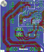
Didn't you already get all of it on there? I though it was just a matter of shifting things around. Seems to be a three partition board, power supply, small signal and high power with protection. Hmm I have not used Eagle PCB, maybe I should give it a try.
I've tried all day, even changing the orientation of the whole board... to have both the DC protection and LM318 PS on sides of the bridges and smoothing caps a slightly bigger PCB is needed (the DC protection takes 1.5*4.0-5.0 cm).
The only way I found so far is the full PCB (0.9.8).
BTW I'm confident this complete configuration would fare well, the 'U' shaped radiating area could be a false problem...
In fact in the little 'U''s branch under half of the LM3886 no important currents should flows.
The LM3886 GND pin is only a reference ground for the mute circuit...
Give a look at the attached zoom picture and help me determining if important currents radiates.
Would that currents be lower if the ground plane under the LM3886 is removed?
Attachments
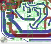
I think most current are going to come from the V+ V- lines through the output 0.47 ohm resistor to the speakers. The OUT line being so close to the LM318 probably is not the best. So what I think is that, on your schematic, anything that is left of the limiter zener should be as far away from the high current section because the LM318 gain is high. All components feeding the inputs should be furthest away. It seems that if the LM3886, c1, c2, c4, 0R47, OUT terminal are moved a bit to the side, they can be further away from the LM318 loop (are those surface mount resistors or limiter diodes beside the OUT trace?)
nFirst of all thanks a lot. ")
I do Agree.
I'll check if it's possible.
I could rotate R3 at the expense of a much longer feedback but distance wouldn't change much.
And/or I can reduce C4 size back to 7.5mm lead spacing gaining 3mm to move R3 toward LM3886.
The original TP layout (excerpt attached) it's not much different in this regard but, obviously, one of my goals is to design a better PCB.
Aren't they?
I thought about it.
It could be possible reducing C1, C2 size back to 10mm diameter gaining 0,5 cm.
But it's worth it?
If you refer to the two ones near the 10pF caps those are MELF resistors.
PS
Rereading the post I see now that some minor component moving is possible... stay tuned... thanks again!
I think most current are going to come from the V+ V- lines through the output 0.47 ohm resistor to the speakers.
I do Agree.
The OUT line being so close to the LM318 probably is not the best. So what I think is that, on your schematic, anything that is left of the limiter zener should be as far away from the high current section because the LM318 gain is high.
I'll check if it's possible.
I could rotate R3 at the expense of a much longer feedback but distance wouldn't change much.
And/or I can reduce C4 size back to 7.5mm lead spacing gaining 3mm to move R3 toward LM3886.
The original TP layout (excerpt attached) it's not much different in this regard but, obviously, one of my goals is to design a better PCB.
All components feeding the inputs should be furthest away.
Aren't they?
It seems that if the LM3886, c1, c2, c4, 0R47, OUT terminal are moved a bit to the side, they can be further away from the LM318 loop
I thought about it.
It could be possible reducing C1, C2 size back to 10mm diameter gaining 0,5 cm.
But it's worth it?
(are those surface mount resistors or limiter diodes beside the OUT trace?)
If you refer to the two ones near the 10pF caps those are MELF resistors.
PS
Rereading the post I see now that some minor component moving is possible... stay tuned... thanks again!
Attachments
Last edited:
Got out my magnifying glass, D1, D2, and the zener are too close to the OUT. If the component/trace runs perpendicular to the high current trace, then it is less effected. Also, field strength reduces by the square with distance.
You can decide where to put you name after the layout is complete.
You can decide where to put you name after the layout is complete.
Last edited:
Got out my magnifying glass, D1, D2, and the zener are too close to the OUT. If the component/trace runs perpendicular to the high current trace, then it is less effected. Also, field strength reduces by the square with distance.
Ok
You can decide where to put you name after the layout is complete.
You can trust me or not but the presence of credits on PCB from the start was a precise request by Mauro...
Rereading the post I see now that some minor component moving is possible... stay tuned... thanks again!
Is it any better?
Take in account that unless Vpp on limiter is higher than 28V that circuit should behave like an open circuit.
Attachments
Even though that might be true, but even a hanging open circuit with only one end connected could effect the sound. That is why the "ground side electrons" thing works. It seems you could still move the limiter to the right.Is it any better?
Take in account that unless Vpp on limiter is higher than 28V that circuit should behave like an open circuit.
I wonder if it's a good idea to have the resistor heat sink against the cap, and also it seems that the real heat sink would interfere with the OUT connector because the relation between the legs and the heat sink is different. What might be a way to solve it is rotate the resistor clockwise by 90 deg and rotate the heat sink counterclockwise 90deg and correct the relation between heat sink and resistor leg. This will give you more room around the OUT connector.
Even though that might be true, but even a hanging open circuit with only one end connected could effect the sound. That is why the "ground side electrons" thing works.
Both ends should be disconnected...
It seems you could still move the limiter to the right.
I thought you asked me to make some more distance between the limiter and the compensation network...
No problem, it's even better.
I wonder if it's a good idea to have the resistor heat sink against the cap, and also it seems that the real heat sink would interfere with the OUT connector because the relation between the legs and the heat sink is different. What might be a way to solve it is rotate the resistor clockwise by 90 deg and rotate the heat sink counterclockwise 90deg and correct the relation between heat sink and resistor leg. This will give you more room around the OUT connector.
I'm not sure that I've understood correctly but I'll give it a try.
I'm not sure that I've understood correctly but I'll give it a try.
Like this?
Attachments
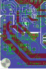
Bigger PCB
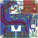
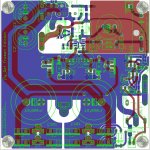
I've managed to buy Eagle Hobbyst Edition so I've made a bigger layout (100x100mm).
Now is all more spaced and 'relaxed' and more components are through hole and there is room to use a screwdriver to fix LM3886 with caps mounted...
Any opinion is welcome
I've managed to buy Eagle Hobbyst Edition so I've made a bigger layout (100x100mm).
Now is all more spaced and 'relaxed' and more components are through hole and there is room to use a screwdriver to fix LM3886 with caps mounted...
Any opinion is welcome
Attachments
Last edited:
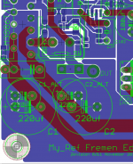
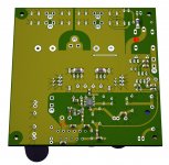
Are all the surface mount components on the same side of the PCB?
Sure, on the bottom one.
Does Eagle PCB allow smooth turns in the traces and teardrop pads?
Smooth turn yes, teardrop pads no, unless you draw them manually on each pad.
Do you think that smooth traces are better? Why?
I don't have any data to prove it. But the more current flows though a wire, keeping smooth traces seems to reduce any reflected energy. Same as water flow or acoustic waves. It usually is not the most important issue, but if you can put that in conveniently, it's better to do so.
I would also still recommend trying to move the limiters away from the OUT path.
I would also still recommend trying to move the limiters away from the OUT path.
Last edited:
Dario,
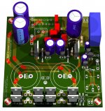
Looks like you have already got a good grasp of this software, and I'm impressed. The design is looking really good for ease of building because it is much less cluttered than your previous attempts.
Now that the board is bigger, is there room enough to lay the resistors near the regulators down instead of standing them upright? Can you make a little more room around the 318? It looks pretty tight for the caps nearby.
Perhaps some of the traces with large radius should be straightened again to make the path shorter. I'm not sure what is really gained by using such large curves, but I think a shorter path is always better. Other than extra length, I do like curves.
Peace,
Tom E
- Status
- This old topic is closed. If you want to reopen this topic, contact a moderator using the "Report Post" button.
- Home
- Amplifiers
- Chip Amps
- My_Ref Fremen Edition - need help on PCB evaluation